
Swapnajit Chakravarty, Min Teng, Reza Safian, Leimeng Zhuang. Hybrid material integration in silicon photonic integrated circuits[J]. Journal of Semiconductors, 2021, 42(4): 041303
- Journal of Semiconductors
- Vol. 42, Issue 4, 041303 (2021)
Abstract
1. Introduction
During the past several decades, silicon photonics has gradually matured into an attractive platform to meet the ever-increasing demands of optical communications[
In this context, silicon and silicon nitride waveguides have experimentally demonstrated low propagation losses, ~0.3 and ~0.06 dB/cm respectively on 300 mm foundry platforms; however other functional challenges remain. Silicon is an indirect bandgap semiconductor and hence does not emit light efficiently at room temperature. Silicon nitride has a very large bandgap and does not emit light either. In contrast, quantum well (QW), quantum-dot (QD) and quantum-dash emitters in direct bandgap III–V semiconductors such as InP and GaAs efficiently emit light at visible, near-infrared and mid-infrared wavelengths. III–V materials can also function as efficient detectors when integrated with ultra-low-loss (ULL) silicon nitride at visible wavelengths. Silicon modulators need to be doped for operation in injection, depletion or accumulation modes that rely on changes in carrier concentration in the waveguiding region with applied bias[
2. Light source integration
Hybrid integration of light sources on chip have been achieved with flip-chip bonding[
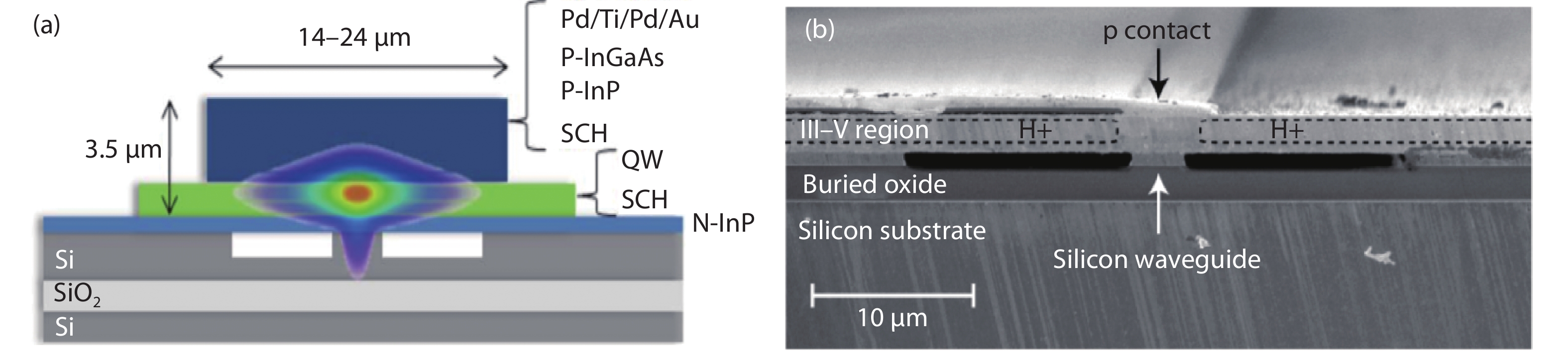
Fig. 1 shows the schematic and scanning electron micrograph (SEM) cross section image of a hybrid III–V laser integrated on a silicon waveguide. The lasing mode is superimposed on the structure in Fig. 1(a). Electrical current flows from the p-contact, through the center of the mesa defined by proton implantation, to the n-contact, while achieving a large overlap with the optical mode. Light generated in the hybrid III–V/Si section is coupled completely into the underlying silicon waveguide via adiabatic multi-level tapering of the III–V epi, as shown in Fig. 2. In Ref. [22], the authors investigated two types of multilevel tapers as shown in Fig. 2. In Fig. 2, the top InP cladding layer of the III–V laser is indicated in blue, the active region of the III–V material is indicated in green, the bottom cladding of the III–V laser and bonding layers are drawn in cyan while the bottom silicon layer is drawn in grey. The chosen designs were made to reduce loss and reflection, and also support fewer higher order modes for efficient light confinement in the fundamental mode. The taper architecture in Fig. 2(a) transferred the power from III–V to silicon more abruptly than the taper design in Fig. 2(b), which was manifested in a higher taper loss in the design in Fig. 2(a) (~0.5 dB).
![]()
Figure 1.(Color online) (a) Schematic of the hybrid laser with the superimposed optical mode. (b) SEM of cross-section of the hybrid laser[
![]()
Figure 2.(Color online) Schematic of mode conversion tapers for coupling light into the silicon waveguide. The silicon waveguide is in gray while different sections of the top III –V layer with different taper lengths are shown in other colors[
Another method popularly adopted in the literature for the hybrid integration of III–V lasers, semiconductor optical amplifiers (SOAs) and III–V photodetectors is micro-transfer printing. Micro-transfer printing (µTP) is a revolutionary heterogeneous integration technology with a high degree of modularity and flexibility[
The principle of micro-transfer printing of III–V gain material onto a silicon passive platform on >8-inch wafer-scale in this program is illustrated in Fig. 3. A poly-dimethyl siloxane (PDMS) stamp with a post array (or a single post) whose size and pitch match those of the device array arranged on the source III–V wafer, is used to pick up and transfer these devices onto a target wafer. The stamp is fabricated through casting PDMS on a Si master mold and after releasing, laminating it on a glass carrier wafer. Over 300 000 printing cycles[
![]()
Figure 3.(Color online) (a, b) Schematic Illustration of micro-transfer printing of III–V gain material on silicon wafers[
The principle of coupling light from the III–V to the silicon section is governed by the supermode theory of the coupled III–V and silicon waveguides presented by Yariv et al. in Ref. [11]. According to this theory and as shown schematically in Fig. 2, it is possible to couple light from the top III–V waveguide to the bottom Si waveguide section simply by tapering the widths of the individual waveguides. As shown in Fig. 4, the upper III–V core-cladding combination and the lower silicon waveguide core with SiO2 cladding form a system of two coupled vertically offset waveguides that are separated by the bonding interface. Such a coupled system of waveguides support two modes with propagation constants β1 and β2 respectively and designated by subscripts odd (o) or even (e) based on their modal symmetry when δ = β1 – β2 = 0.
![]()
Figure 4.(Color online) Schematic representation of the two supermodes, designated by
As observed in Fig. 4, by changing the δ parameter by controlling the widths of the individual waveguides as schematically illustrated in Fig. 2, the particular waveguide whether III–V or silicon in which the odd or even mode field is concentrated is determined. For the even supermode, in one roundtrip, light starts in the III–V waveguide where it is amplified, enters the adiabatic transformer section where δ changes from δ < 0 to δ > 0 by increasing the Si waveguide width and simultaneously decreasing the III–V width thereby transferring the mode energy to the bottom Si waveguide where it is partially reflected towards the left high reflection coating facet on the left of the III–V waveguide, thereby completing one roundtrip. The odd mode E0 being primarily confined in the lower silicon waveguide in the lasing section on the left image in Fig. 4, has a high lasing threshold and is thus prevented from lasing.
IMEC’s iSiPP50G platform has silicon ridge waveguides of thickness 220 nm with demonstrated propagation loss ~0.3 dB/cm. For efficient coupling from III–V to silicon via the adiabatic tapering concept illustrated in Fig. 4, it is necessary to have an intermediate poly-Si interface of thickness 160 nm, which is also available in the iSiPP50G process, as shown in Figs. 5(a) and (b). The lower waveguide in Fig. 5 is essentially 160 nm of poly-Si (in green) on 220 nm device silicon (in purple) in a SOI wafer. Figs. 5(A)–5(H) shows the evolution of the optical mode from a typical laser epi stack in the O-band to the underlying poly-Si/Si waveguide, with the corresponding cross-sections at which the mode profiles are obtained being shown in Fig. 5(b). The III–V epi section can be patterned into a ridge laser with air cladding or a buried heterostructure laser with Fe:InP cladding when high power is desired. As noted in Figs. 6(a) and 6(b), in both configurations, EigenMode Expansion (EME) simulations in the Lumerical MODE indicate that the coupling taper length increases with increasing thickness of the III–V cladding region separating the III–V core region from the poly-silicon surface. Simulations were also performed for various ridge widths in the buried heterostructure configuration, as shown in Fig. 6(c). Once light is coupled into the passive poly-Si/silicon region, as shown in Fig. 7(a), the poly-Si layer is tapered to couple the even mode to the fundamental transverse electric (TE) mode in the silicon passive waveguide, as shown in Fig. 7(b). IMEC’s iSiPP50G platform also enables co-integration of silicon and silicon nitride waveguides. Fig. 7(c) shows that by suitably designing the taper in both silicon and silicon nitride in opposite directions, the fundamental TE mode can be coupled entirely from the silicon with 220 nm thickness to 400 nm silicon nitride thickness, separated by an oxide thickness ~200 nm.
![]()
Figure 5.(Color online) Schematic (a) top view and (b) side view of the III–V light emitting heterostructure with Fe:InP cladding in the buried heterostructure configuration integrated on a SOI wafer with an intermediate polysilicon layer (in green). A dual taper configuration is shown in the adiabatic mode transformation region where the laser ridge as well as the underlying polysilicon layers are tapered. The mode evolution of the fundamental TE mode from the gain region to the underlying silicon-poly-Si waveguide is shown in (A)–(H) with the corresponding cross-sections demarcated in (b).
![]()
Figure 6.(Color online) Coupling efficiency vs taper length as function of bottom cladding thickness for (a) air clad ridge laser and (b) buried heterostructure laser and (c) as a function of buried ridge width.
![]()
Figure 7.(Color online) (a) Schematic cross-section of the hybrid laser/light emitter bonded to polysilicon (in green) on device silicon (in purple). Coupling efficiency versus taper length for coupling from (b) poly-Si to 220 nm silicon, and (c) from 220 nm silicon to 400 nm silicon nitride for various oxide gaps between silicon and silicon nitride as indicated in (a).
The hybrid integration scheme of the III–V gain section to silicon passives offers a significant device processing advantage compared to III–V lasers. As shown schematically in Fig. 3(c), front and rear distributed Bragg reflector (DBR) gratings can be defined in the silicon in standard CMOS processing to define Bragg reflectors with any desired reflectivity. Figs. 8(a) and 8(b) shows a typical reflectivity spectra for a different number of grating periods and tooth depths. In addition, hybrid integration allows the Bragg grating tunable sections in III–V lasers from the gain region. Fig. 8(c) shows typical tunable spectra from a system of two coupled Vernier ring resonators in the O-Band. Individual ring resonances can be thermo-optically tuned to tune the lasing wavelength of the hybrid laser. Similar demonstrations have been done in the C-band in Ref. [14].
![]()
Figure 8.(Color online) Reflectivity spectra of DBR reflectors for gratings with (a) etch depth of 100nm and 3600 periods with period
3. Ferroelectric modulator integration with silicon PICs
Heterogeneous integration techniques have led to the emergence of ultra-compact thin-film lithium niobate (TFLN) electro-optic (EO) modulators on silicon substrates. Several high performance TFLN EO modulators with 3 dB bandwidths up to ~100 GHz have been demonstrated[
Various TFLN hybrid integration strategies have been reported in the literature. While etched LN on lithium-niobate-on-insulator (LNOI) wafers are being demonstrated elsewhere, Figs. 9(a) and 9(b) show schematics of two architectures for integration of unetched slab TFLN with embedded and un-embedded electrodes respectively.
![]()
Figure 9.(Color online) Schematic of hybrid TFLN integrated with silicon PICs with (a) embedded electrodes[
The steps in the fabrication/hybrid integration of TFLN with silicon waveguides and embedded electrodes have been reported in Ref. [27]. In Fig. 10, we show the steps in the hybrid integration with electrodes not embedded in the silicon PIC.
![]()
Figure 10.(Color online) Steps in the hybrid integration of TFLN on silicon or silicon nitride PICs.
The silicon or silicon nitride waveguides in Mach–Zehnder interferometer configurations, with grating couplers and other passive waveguide components, are patterned in a full wafer or multi-project wafer (MPW) which runs in a standard 200 or 300 mm foundry using 193 nm lithography. The patterned die/wafer is planarized with silicon dioxide (SiO2) to have a surface roughness compatible with high yield bonding as shown in Fig. 1(d). Thin film lithium niobate on insulator (LNOI) wafers are cut into dies of sizes compatible with modulator lengths (~5 mm to 2 cm) followed by deposition of SiO2 and polishing for a die–die bonding compatible surface as shown in Fig. 1(e). Since LN is not a foundry compatible material, subsequent post-processing is done in a custom semiconductor microfabrication facility with steps involving the removal of the silicon handle and SiO2 from the LNOI die [Figs. 1(h) and 1(i)] and traveling wave modulator (TWM) electrode definition by metal-lift-off [Fig. 1(j)].
A III–V gain medium can be bonded or transfer printed either before or after the metal lift-off step, as shown in Fig. 11, wherein the silicon or silicon nitride waveguides in those sections are adiabatically tapered as described in Sec. 2 to achieve full integration. One may note that the grating coupler output in Fig. 11 can be substituted by integrated photodetectors that receive light guided by the silicon/silicon nitride waveguides via adiabatically tapered waveguides.
![]()
Figure 11.(Color online) Steps in the hybrid integration of a III–V laser with silicon in a hybrid TFLN on silicon or silicon nitride PIC.
For EO modulators, a few significant parameters of interest are the 3 dB RF bandwidth, the Vπ-L, the RF propagation loss and the optical waveguide propagation loss along with other metrics such as insertion loss, ripple, temperature dependence etc. In both structures with embedded and un-embedded electrodes shown in Fig. 9, the bonding interface is shown in red and is a significant determining factor for the Vπ-L parameter. Fig. 12 shows a typical refractive index profile and mode profile for a 400 nm thin LN slab on a 220 × 200 nm2 silicon nitride waveguide, separated by an oxide bonding interface ~50 nm.
![]()
Figure 12.(Color online) (a) Refractive index profile and (b) optical mode profile of the fundamental TE mode in a thin film ~400 nm LN bonded to a silicon waveguide 240 × 220 nm2 separated by 100 nm SiO2 interface. The top cladding is air.
As observed in Fig. 12, the optical mode profile in the modulator section spreads in the slab lithium niobate. While alternate designs with etched LN strongly confines the mode, as will be shown later in Fig. 14, we observe from Tables 1 and 2 in Fig. 13 that the optical overlap integral with the adjacent electrodes and the consequent proximity induced optical loss sets a lower limit to the minimum distance between the ground and signal electrodes in the traveling wave modulator. By setting this lower limit as 1 dB/cm, we observe that the thickness of the gap interface oxide, indicated in red in Fig. 9, plays a significant role such hybrid integration.
![]()
Figure 13.(Color online) Tables indicating optical propagation loss contribution from the overlap of the propagating optical mode with the ground and signal electrodes as a function of interface oxide thickness (vertical axis) and spacing between ground and signal electrode (horizontal axis) for hybrid traveling wave modulator configuration with (a) an embedded electrode and (b) an un-embedded electrode.
![]()
Figure 14.(Color online) (a) Cross-section schematic of etched LN integrated with silicon PIC. (b) Optical propagation loss contribution from the overlap of the propagating optical mode with the ground and signal electrodes as a function of interface oxide thickness (vertical axis) and spacing between ground and signal electrode (horizontal axis) for hybrid traveling wave modulator configuration.
From a fabrication standpoint, an oxide interface gap of dimensions shown in Fig. 13 imposes stringent bonding interface requirements. With an oxide interface gap of 50 nm between the top of the silicon and the bottom of the TFLN, a minimum spacing of 10 μm is required between the ground and signal electrodes, so that the optical propagation loss (excluding the material loss, surface roughness loss) simply due to the overlap of the optical mode with the electrodes is less than 1 dB/cm. Simulations indicate that the Vπ-L increases to 3.28 and 3.92 V·cm respectively for embedded and unembedded electrodes case, versus ~2 V·cm which would have been possible if the electrodes were 5 μm apart. While details will be covered elsewhere, it may be noted that the RF loss is higher and RF bandwidths significantly lower in the case with embedded electrodes versus unembedded electrodes.
It is possible to overcome the stringent oxide thickness limitations with TFLN slab structures presented previously, however, that will be the subject of a different paper. Another option to overcome such stringent limitations is to bond an etched LN film in Fig. 10(e) in which case, the cross-section profile of the bonded etched LN film in the modulator section is as shown in Fig. 14.
As observed in Fig. 14, the interface oxide thickness stringency is significantly relaxed whilst also enabling ground-signal electrode spacing ~4 μm thereby enabling low Vπ-L.
In such hybrid architectures, light initially coupled into a silicon or silicon nitride waveguide via grating couplers (as shown in Fig. 12) is coupled to the etched LN film by adiabatic tapering of both the silicon waveguide and the TFLN so that nearly 100% light is coupled for propagation in the rib etched LN over a coupling length ~100 μm. In Fig. 15, a fraction of the propagating mode in the modulator section is still in the silicon; however one can taper the silicon waveguide width to zero in which case the mode would reside entirely in the rib etched LN.
![]()
Figure 15.(Color online) Evolution of the optical mode as it couples from the silicon to the etched TFLN in
The adiabatic tapering architecture is also robust to misalignment. As demonstrated elsewhere with respect to the transfer printed alignment of III–V lasers to a passive silicon waveguide, we observe in Fig. 16 the simulated optical mode profile for ~500 nm misalignment while bonding the etched LN to the silicon PIC. We observe in Fig. 16 that nearly 100% of the propagating optical mode initially in silicon can be coupled to the etched TFLN film bonded above, the misalignment offset being accounted for during fabrication by a slightly longer taper length ~500 μm.
![]()
Figure 16.(Color online) (a) Schematic cross-section assuming the TFLN slab has a misalignment offset of 500 nm perpendicular to the waveguide, when bonding. Mode profiles in the (b) adiabatic coupling section and (c) TFLN in the modulator section. (d) Coupling efficiency as a function of adiabatic taper length when waveguides are misaligned.
4. Conclusion
In summary, in this paper, we have reviewed the basic principles of hybrid integration of different materials with silicon PICs, to attribute functionalities unachievable in silicon or Group IV semiconductors alone. III–V materials have been efficiently integrated with silicon by various methods including bonding and transfer printing to function as gain media for lasers and SOAs, and as efficient photodetectors. While III–V materials are also promising candidates as modulators by virtue of their linear and non-linear electro-optic characteristics, low-loss ferroelectric modulator integration with silicon PICs is also reaching advanced maturity. In addition to thin film lithium niobate (TFLN) referenced here, similar efforts are ongoing at IMEC and elsewhere towards integration of barium titanate (BTO) that have demonstrated superior EO-coefficients[
References
[1] C R Doerr. Silicon photonic integration in telecommunications. Front Phys, 3, 37(2015).
[2] W Q Xie, T Komljenovic, J X Huang et al. Heterogeneous silicon photonics sensing for autonomous cars. Opt Express, 27, 3642(2019).
[3] D Marpaung, J P Yao, J Capmany. Integrated microwave photonics. Nat Photonics, 13, 80(2019).
[4] A W Elshaari, W Pernice, K Srinivasan et al. Hybrid integrated quantum photonic circuits. Nat Photonics, 14, 285(2020).
[5] L Liu, J van Campenhout, G Roelkens et al. Carrier-injection-based electro-optic modulator on silicon-on-insulator with a heterogeneously integrated III-V microdisk cavity. Opt Lett, 33, 2518(2008).
[6] G T Reed, D J Thomson, F Y Gardes et al. High-speed carrier-depletion silicon Mach-Zehnder optical modulators with lateral PN junctions. Front Phys, 2, 77(2014).
[7] K Debnath, D J Thomson, W W Zhang et al. All-silicon carrier accumulation modulator based on a lateral metal-oxide-semiconductor capacitor. Photonics Res, 6, 149(2018).
[8] C Wang, M Zhang, X Chen et al. Integrated lithium niobate electro-optic modulators operating at CMOS-compatible voltages. Nature, 562, 101(2018).
[9] F Eltes, C Mai, D Caimi et al. A BaTiO3-based electro-optic pockels modulator monolithically integrated on an advanced silicon photonics platform. J Light Technol, 37, 1456(2019).
[10] X L Wang, C Y Lin, S Chakravarty et al. Effective in-device
[11] A Yariv, X K Sun. Supermode Si/III-V hybrid lasers, optical amplifiers and modulators: A proposal and analysis. Opt Express, 15, 9147(2007).
[12] S Tanaka, S H Jeong, S Sekiguchi et al. High-output-power, single-wavelength silicon hybrid laser using precise flip-chip bonding technology. Opt Express, 20, 28057(2012).
[13] Q Li, K M Lau. Epitaxial growth of highly mismatched III-V materials on (001) silicon for electronics and optoelectronics. Prog Cryst Growth Charact Mater, 63, 105(2017).
[14] G Roelkens, A Abassi, P Cardile et al. III-V-on-silicon photonic devices for optical communication and sensing. IEEE Photonics J, 3, 969(2015).
[15] G Roelkens, D van Thourhout, R Baets et al. Laser emission and photodetection in an InP/InGaAsP layer integrated on and coupled to a silicon-on-insulator waveguide circuit. Opt Express, 14, 8154(2006).
[16] T Tatsumi, K Tanabe, K Watanabe et al. 1.3 μm InAs/GaAs quantum dot lasers on Si substrates by low-resistivity, Au-free metal-mediated wafer bonding. J Appl Phys, 112, 033107(2012).
[17] T Hong, G Z Ran, T Chen et al. A selective-area metal bonding InGaAsP–Si laser. IEEE Photonics Technol Lett, 22, 1141(2010).
[18] D Liang, J E Bowers. Highly efficient vertical outgassing channels for low-temperature InP-to-silicon direct wafer bonding on the silicon-on-insulator substrate. J Vac Sci Technol B, 26, 1560(2008).
[19] J Zhang, G Muliuk, J Juvert et al. III-V-on-Si photonic integrated circuits realized using micro-transfer-printing. APL Photonics, 4, 110803(2019).
[20] C O de Beeck, B Haq, L Elsinger et al. Heterogeneous III-V on silicon nitride amplifiers and lasers via microtransfer printing. Optica, 7, 386(2020).
[21] H Park, A Fang, S Kodama et al. Hybrid silicon evanescent laser fabricated with a silicon waveguide and III-V offset quantum wells. Opt Express, 13, 9460(2005).
[22] G Kurczveil, P Pintus, M J R Heck et al. Characterization of insertion loss and back reflection in passive hybrid silicon tapers. IEEE Photonics J, 5, 6600410(2013).
[23] M A Meitl, Z T Zhu, V Kumar et al. Transfer printing by kinetic control of adhesion to an elastomeric stamp. Nat Mater, 5, 33(2006).
[24] X X Wang, P O Weigel, J Zhao et al. Achieving beyond-100-GHz large-signal modulation bandwidth in hybrid silicon photonics Mach Zehnder modulators using thin film lithium niobate. APL Photonics, 4, 096101(2019).
[25] Y Tang, J D Peters, J E Bowers. Over 67 GHz bandwidth hybrid silicon electroabsorption modulator with asymmetric segmented electrode for 1.3 μm transmission. Opt Express, 20, 11529(2012).
[26] E Menard, K J Lee, D Y Khang et al. A printable form of silicon for high performance thin film transistors on plastic substrates. Appl Phys Lett, 84, 5398(2004).
[27] R Safian, M Teng, L M Zhuang et al. Foundry-compatible thin film lithium niobate modulator with RF electrodes buried inside the silicon oxide layer of the SOI wafer. Opt Express, 28, 25843(2020).
[28] M Ayata, Y Fedoryshyn, W Heni et al. High-speed plasmonic modulator in a single metal layer. Science, 358, 630(2017).
[29] M Thomaschewski, V A Zenin, C Wolff et al. Plasmonic monolithic lithium niobate directional coupler switches. Nat Commun, 11, 1(2020).


Set citation alerts for the article
Please enter your email address

© Copyright 2018-2021 | Chinese Laser Press. All Rights Reserved 沪ICP备15018463号-20