• Chinese Optics Letters
  • Vol. 21, Issue 1, 011301 (2023)
Han Ye1、2、*, Qin Han1、2、3, Shuai Wang1, Feng Xiao1、4, Fan Xiao1、4, Yimiao Chu1、4, and Liyan Geng1
Author Affiliations
  • 1State Key Laboratory of Integrated Optoelectronics, Institute of Semiconductors, Chinese Academy of Sciences, Beijing 100083, China
  • 2Center of Materials Science and Optoelectronics Engineering, University of Chinese Academy of Sciences, Beijing 100049, China
  • 3School of Electronic, Electrical and Communication Engineering, University of Chinese Academy of Sciences, Beijing 100049, China
  • 4College of Materials Science and Optoelectronic Technology, University of Chinese Academy of Sciences, Beijing 100049, China
  • show less
    DOI: 10.3788/COL202321.011301 Cite this Article Set citation alerts
    Han Ye, Qin Han, Shuai Wang, Feng Xiao, Fan Xiao, Yimiao Chu, Liyan Geng. Fabrication and photo-response of monolithic 90° hybrid-photodetector array chip for QPSK detection[J]. Chinese Optics Letters, 2023, 21(1): 011301 Copy Citation Text show less
    Cross-section SEM image of epitaxial layers after regrowth.
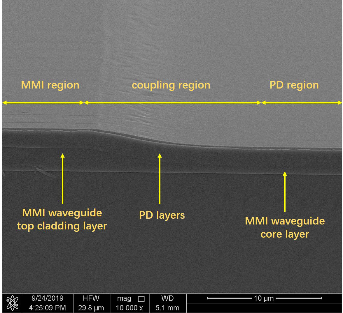
    Fig. 1. Cross-section SEM image of epitaxial layers after regrowth.
    PD jointed to the hybrid waveguide 3D image.
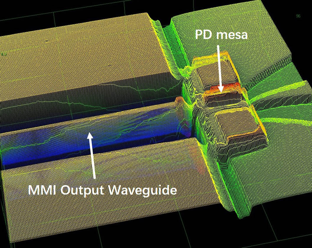
    Fig. 2. PD jointed to the hybrid waveguide 3D image.
    Microscope photo of the fabricated monolithic chip.
    Fig. 3. Microscope photo of the fabricated monolithic chip.
    Dark current of the PD array.
    Fig. 4. Dark current of the PD array.
    Responsivities and excess loss of the monolithic chip.
    Fig. 5. Responsivities and excess loss of the monolithic chip.
    CMRR of the monolithic chip.
    Fig. 6. CMRR of the monolithic chip.
    Spectral response of the monolithic chip integrated with the splitter.
    Fig. 7. Spectral response of the monolithic chip integrated with the splitter.
    Phase deviation of the monolithic chip.
    Fig. 8. Phase deviation of the monolithic chip.
    Simulated phase deviation with fabrication error.
    Fig. 9. Simulated phase deviation with fabrication error.
    Simulated excess loss with fabrication error.
    Fig. 10. Simulated excess loss with fabrication error.
    Input/Output waveguide width2.0 µm
    Waveguide separation5.0 µm
    Taper end width3.6 µm
    Taper length50 µm
    MMI region length810 µm
    MMI region width20 µm
    Table 1. Parameters of the 90° Hybrid
    Material CompositionDoping Type and Density [cm3]Thickness [nm]
    In0.53Ga0.47AsP, 1×101850
    InPP, 2×1017300
    InGaAsP (graded)P, 1×101640
    In0.53Ga0.47As (absorption layer)N, 1×1016560
    InGaAsP (graded)N, 2×101740
    InGaAsP (Q1.065)N, 3×1018500
    Table 2. Parameters of the Evanescent Photodetector
    MMI region length95 µm
    MMI region width10 µm
    Delay line radius550 µm
    Delay line length difference172.24 µm
    Table 3. Parameters of the 1 × 2 Splitter
    Han Ye, Qin Han, Shuai Wang, Feng Xiao, Fan Xiao, Yimiao Chu, Liyan Geng. Fabrication and photo-response of monolithic 90° hybrid-photodetector array chip for QPSK detection[J]. Chinese Optics Letters, 2023, 21(1): 011301
    Download Citation