
Han Ye, Qin Han, Shuai Wang, Feng Xiao, Fan Xiao, Yimiao Chu, Liyan Geng, "Fabrication and photo-response of monolithic 90° hybrid-photodetector array chip for QPSK detection," Chin. Opt. Lett. 21, 011301 (2023)
- Chinese Optics Letters
- Vol. 21, Issue 1, 011301 (2023)
Abstract
1. Introduction
Encouraged by the high-speed data transmission demand of the developing 5G and the upcoming 6G optical communication systems, a big surge in the aggregate data transfer rate in optical networks will be expected in the near future. The coherent optical transmission technology, nowadays standard in the long-haul fiber-optic networks, will be further ameliorated into shorter distance applications such as metropolitan areas, access networks, or even data centers[1,2]. Enabled by the high-order (de)modulation formats scheme targeting both amplitude and phase of the optical carrier, it could conveniently expand data bitrate by-fold without remarkable increase in optic module speed[3]. One of the most popular and widely used formats is quadrature phase-shift keying (QPSK). It utilizes four quadrature phase states to encode 2 bit information into one symbol and doubles the transmission rate accordingly with a higher receiver sensitivity as well. Early researches on transmission link performance and signal processing methods have proven the effectiveness and feasibility of the format[4–6].
On the other hand, higher port density and pluggable optical modules in such networks require miniaturization of optical components for less power consumption and optical coupling loss, where integrated devices and modules are obviously a better choice than assembled ones. Many monolithic coherent transceivers have been reported for C-band applications, with low excess loss of 1 dB[7], high responsivity of 70 mA/W[8], and high channel speed[9]. Other novel types of hybrids have also been proposed for compact size and wide operation wavelength ranges[10,11]. We have also recently designed and fabricated an InP-based 90° hybrid for QPSK at the C-band[12] with comparable phase and common mode rejection ratio (CMRR) characteristics.
In this Letter, a four-channel evanescent photodetector (PD) array is further monolithically integrated to the 90° hybrid with its operation wavelength range adjusted to the wider L-band. The chip is fabricated by the metal organic chemical vapor deposition (MOCVD) regrowth technology, and its photo-response is characterized. The monolithic chip shows a CMRR better than 13.6 dB, a phase deviation within
Sign up for Chinese Optics Letters TOC. Get the latest issue of Chinese Optics Letters delivered right to you!Sign up now
2. Device Design
The monolithic chip consists of a 90° hybrid based on the
| Input/Output waveguide width | 2.0 µm |
| Waveguide separation | 5.0 µm |
| Taper end width | 3.6 µm |
| Taper length | 50 µm |
| MMI region length | 810 µm |
| MMI region width | 20 µm |
Table 1. Parameters of the 90° Hybrid
A taper of linearly varied width is inserted between each input/output waveguide and the MMI region for less phase deviation sensitivity on the MMI region width. The MMI region length is estimated by the self-imaging principle for the four-fold general imaging situation[13]:
The PD structure layers are designed to be regrown on the MMI core layer to collect optical power by evanescent field coupling to the absorption layer. Details are listed in Table 2. The active area of each PD is
| Material Composition | Doping Type and Density [ | Thickness [nm] |
|---|---|---|
| P, | 50 | |
| InP | P, | 300 |
| InGaAsP (graded) | P, | 40 |
| N, | 560 | |
| InGaAsP (graded) | N, | 40 |
| InGaAsP (Q1.065) | N, | 500 |
Table 2. Parameters of the Evanescent Photodetector
An MZ
| MMI region length | 95 µm |
| MMI region width | 10 µm |
| Delay line radius | 550 µm |
| Delay line length difference | 172.24 µm |
Table 3. Parameters of the 1 × 2 Splitter
3. Chip Fabrication
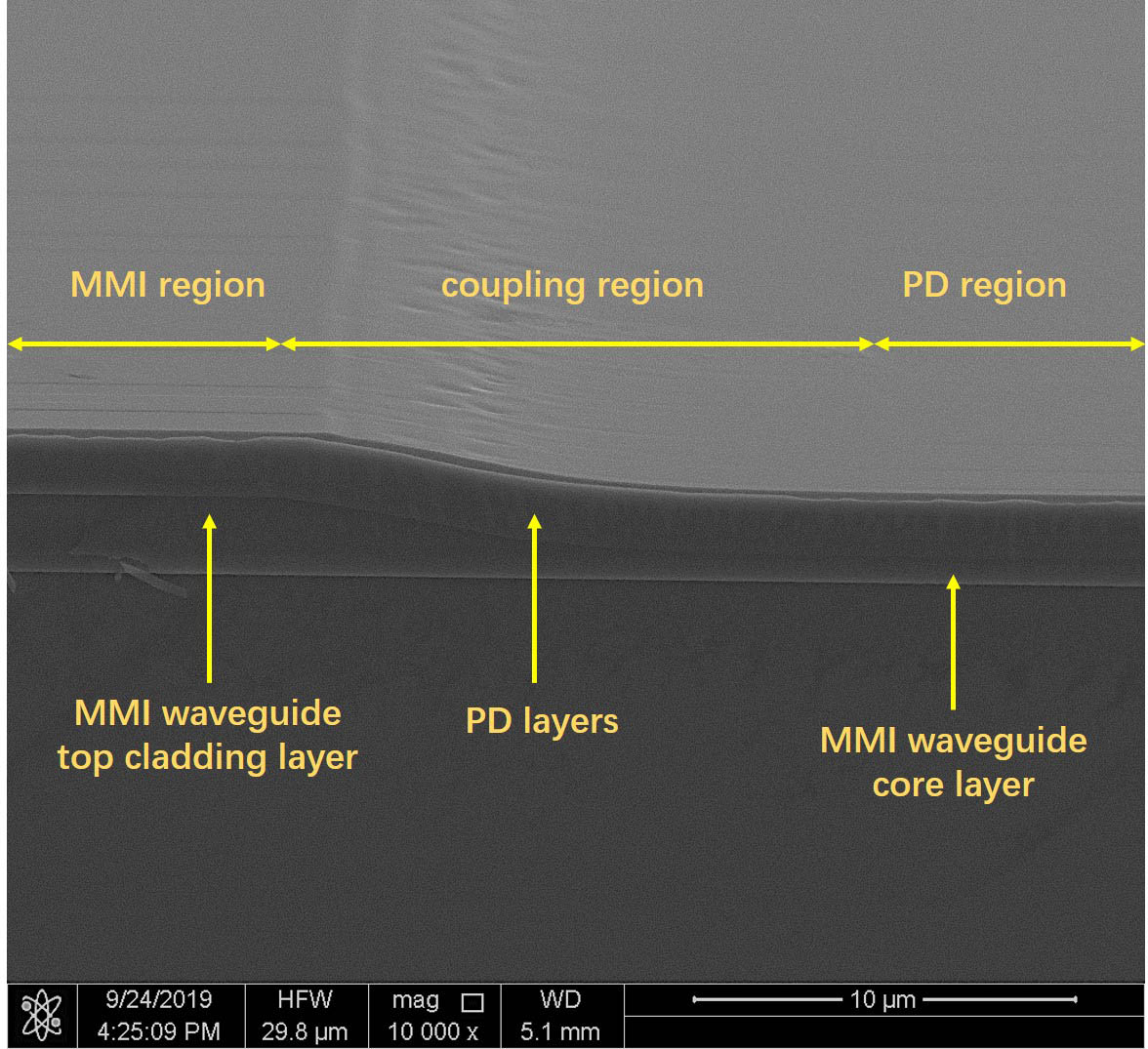
Fabrication of the monolithic chip starts with waveguide layers growth by MOCVD. Then, the top cladding layer in the PD region is removed by chemical etching using hydrochloric and phosphoric acid solutions. The patterned substrate then undergoes a second MOCVD for whole area PD layers growth. Figure 1 illustrates the epitaxial layer structure after regrowth. The PD layers cover the whole hybrid and splitter regions over the top cladding layer, the coupling region with gradually thinning cladding layer, and the core layer at the PD region. Two inductively coupled plasma (ICP) etching steps are conducted successively to define first the p-i-n junction mesa and then the N-contact mesa. The N-contact mesa front edge has extended 8 µm before the junction mesa into the coupling region to prevent high optical coupling loss as previously demonstrated[15]. PD layers elsewhere are redundant and etched out completely in the process. Metallization of contacts are realized by lifting off the Au/Ge/Ni alloy film for the N type and chemically etching the Ti/Au film for the P type, followed by a rapid 1 min thermal annealing at 410°C. A thick 700 nm
![]()
Figure 1.Cross-section SEM image of epitaxial layers after regrowth.
![]()
Figure 2.PD jointed to the hybrid waveguide 3D image.
![]()
Figure 3.Microscope photo of the fabricated monolithic chip.
4. Result Discussion
Measurement of the monolithic chip is conducted on a high-precision test platform using a tunable laser at TE polarization. The dark current of the each PD in the array is measured to be uniformly lower than 100 nA at
![]()
Figure 4.Dark current of the PD array.
![]()
Figure 5.Responsivities and excess loss of the monolithic chip.
The CMRR represents this imbalance of responsivity and is defined by
![]()
Figure 6.CMRR of the monolithic chip.
The excess loss of the monolithic chip is estimated. Apart from the 6 dB intrinsic loss of an ideal four-fold imaging for each hybrid input, an excess loss also exists to represent an extra loss of on-chip passive components compared to a straight waveguide, which contains optical scattering loss from but not limited to the imperfect imaging, the waveguide bending, or other kinds of waveguide shapes and sizes. A waveguide-integrated PD (WG-PD) is fabricated on the same wafer, by the same method, in the same process for this estimation. The waveguide length is the same as the total length of the hybrid and the splitter. By deducting the WG-PD external responsivity (blue square in Fig. 5) from the total responsivity (red line in Fig. 5) of the monolithic chip, losses from the fiber end coupling could be eliminated. Consequently, a small excess loss of 0.85 dB is obtained (green diamond in Fig. 5) for almost the entire L-band. We believe that the bending loss of the designed extreme slim 2 µm waveguide and the scattering of the rough MMI sidewall are the main sources of this loss.
The phase deviation of the monolithic chip could be deduced from the spectral response measurement result with the integrated
![]()
Figure 7.Spectral response of the monolithic chip integrated with the splitter.
Phase distance between channels is calculated by the peak or valley distance in the spectrum:
![]()
Figure 8.Phase deviation of the monolithic chip.
Measurement results include both fabrication and measurement errors. For one thing, the inaccurate graphic transfer process may lead to waveguide size distortion, in which width variation is the primary contributor to the larger phase deviation. Supplementary simulations are conducted for phase deviation and excess loss of the hybrid and power splitter, with a 300 nm width increase for waveguides considered. Simulation results by the finite-difference-time-domain propagation method show a phase deviation larger than 5° near 1585 nm in Fig. 9 and an excess loss decreasing from 0.8 dB to 0.05 dB in Fig. 10 for the hybrid at the 40 nm span mentioned above. The
![]()
Figure 9.Simulated phase deviation with fabrication error.
![]()
Figure 10.Simulated excess loss with fabrication error.
For the other thing, measurement errors will result in an overestimated phase deviation as well, since the phase distance between channels is deduced from peak/valley wavelengths in the spectral response curves. Therefore, any discrepancy of the test laser wavelength will lead to extra calculated phase deviations, which might come from limited equipment accuracy. In this work,
Provided that the more delicate e-beam lithography and a finer tunable laser for chip fabrication and measurement are to be adopted, a better phase deviation controlled into
5. Conclusion
A 90° hybrid monolithic with a PD array is fabricated and characterized in the L-band. The evanescent four-PDs array is monolithically integrated by MOCVD regrowth technology to ensure an intact waveguide epitaxial structure for the passive hybrid, hence a small excess loss of 0.85 dB. Still, the PD array shows a similar dark current density similar to the one without regrowth and a uniform dark current lower than 100 nA at
The bandwidth of the PD array reaches 15 GHz for each PD unit, which is yet to be promoted for high-speed detection. The primary cause is the relatively low density of
Despite all that, the integration method in this work still proves feasible for a coherent PD chip, which could conveniently include more passive structures like the MZ splitter. The chip integrated with the MZ splitter could potentially constitute together as the core module in the differential QPSK (DQPSK) receiver, where the delay line is 1 bit long in time to realize self-homodyne photo-detection with no need for local oscillators. Furthermore, the DQPSK receiver could also possibly convert DQPSK signals to 4-ary pulse amplitude modulation (PAM4) ones and hopefully cut down power consumption[18]. Higher level integration of the basic chip structure in this work could be expected to realize more multiplexing dimensions, larger channel number, and higher information transmission rate.
References
[1] X. Zhou, H. Liu, R. Urata, S. Zebian. Scaling large data center interconnects: challenges and solutions. Opt. Fiber Technol., 44, 61(2018).
[2] P. J. Winzer, R. J. Essiambre. Advanced modulation formats for high-capacity optical transport networks. J. Lightwave Technol., 24, 4711(2006).
[3] E. Lach, W. Idler. Modulation formats for 100G and beyond. Opt. Fiber Technol., 17, 377(2011).
[4] Y. Feng, H. Wen, H. Y. Zhang, X. P. Zheng. 40-Gb/s PolMux-QPSK transmission using low-voltage modulation and single-ended digital coherent detection. Chin. Opt. Lett., 8, 976(2010).
[5] S. W. Lu, Y. Zhou, F. N. Zhu, J. F. Sun, Y. Yang, R. Zhu, S. N. Hu, X. X. Zhang, X. L. Zhu, X. Hou, W. B. Chen. Digital-analog hybrid optical phase-lock loop for optical quadrature phase-shift keying. Chin. Opt. Lett., 18, 090602(2020).
[6] J. K. Perin, A. Shastri, J. M. Kahn. DSP-free coherent receivers for data center links. Proceedings of Optical Fiber Communication Conference, Tu2C.1(2018).
[7] T. Kikuchi, H. Yagi, N. Inoue, R. Masuyama, T. Katsuyama, K. Uesaka, Y. Yoneda, H. Shoji. High-responsivity of InP-based photodiodes integrated with 90° hybrid by low excess loss MMI design over wide wavelength range. Proceedings of Photonics Conference, 370(2014).
[8] M. Takechi, Y. Tateiwa, M. Kurokawa, Y. Fujimura, H. Yagi, Y. Yoneda. 64 GBaud high-bandwidth micro intradyne coherent receiver using high-efficiency and high-speed InP-based photodetector integrated with 90° hybrid. Proceedings of Optical Fiber Communication Conference, Th1A.2(2017).
[9] P. Runge, G. Zhou, T. Beckerwerth, F. Ganze, S. Keyvaninia, S. Seifert, W. Ebert, S. Mutschall, A. Seeger, M. Schell. Waveguide integrated balanced photodetectors for coherent receivers. IEEE J. Sel. Top. Quantum Electron., 24, 610037(2017).
[10] S. H. Jeong, K. Morito. Compact optical 90° hybrid employing a tapered 2 × 4 MMI coupler serially connected by a 2 × 2 MMI coupler. Opt. Express, 18, 4275(2010).
[11] Z. Wang, Y. M. Zhai, Y. Q. Lu, J. Xu, X. H. Sun, J. Wang. Compact optical 90° hybrid based on hybrid plasmonic multimode interferometer. Opt. Commun., 426, 99(2018).
[12] Z. Q. Lu, Q. Han, H. Ye, S. Wang, F. Xiao. Manufacturing tolerance analysis of deep-ridged 90° hybrid based on InP 4 × 4 MMI. Photonics, 7, 26(2020).
[13] M. Bachmann, P. A. Besse, H. Melchior. General self-imaging properties in N × N multimode interference couplers including phase relations. Appl. Opt., 33, 3905(1994).
[14] L. B. Soldano, E. C. M. Pennings. Optical multi-mode interference devices based on self-imaging: principles and applications. J. Lightwave Technol., 13, 615(1995).
[15] H. Ye, Q. Han, Q. Q. Lv, P. Pan, J. M. An, X. H. Yang. Monolithic integration of an InP-based 4 × 25 GHz photodiode array to an O-band arrayed waveguide grating demultiplexer. Opt. Laser Technol., 97, 290(2017).
[16] H. Ye, Q. Han, Q. Q. Lv, P. Pan, J. M. An, X. H. Yang, Y. B. Wang, R. R. Liu. 4 × 25 GHz uni-traveling carrier photodiode arrays monolithic with InP-based AWG demultiplexers using the selective area growth technique. Chin. Opt. Lett., 8, 082301(2017).
[17] S. Q. Liu, X. H. Yang, Y. Liu, B. Li, Q. Han. Design and fabrication of a high-performance evanescently coupled waveguide photodetector. Chin. Phys. B, 22, 108503(2013).
[18] T. Amano, H. Kishikawa, N. Goto. Simple DQPSK receiver based on format conversion from DQPSK to 4PAM by using a delay line interferometer and a photo detector. Proceedings of Opto-Electronics and Communications Conference(2020).


Set citation alerts for the article
Please enter your email address

© Copyright 2018-2021 | Chinese Laser Press. All Rights Reserved 沪ICP备15018463号-20