Abstract
High-performance germanium (Ge) waveguide photodetectors are designed and fabricated utilizing the inductive-gain-peaking technique. With the appropriate integrated inductors, the 3-dB bandwidth of photodetectors is significantly improved owing to the inductive-gain-peaking effect without any compromises to the dark current and optical responsivity. Measured 3-dB bandwidth up to 75 GHz is realized and clear open eye diagrams at 64 Gbps are observed. In this work, the relationship between the frequency response and large signal transmission characteristics on the integrated inductors of Ge waveguide photodetectors is investigated, which indicates the high-speed performance of photodetectors using the inductive-gain-peaking technique.High-performance germanium (Ge) waveguide photodetectors are designed and fabricated utilizing the inductive-gain-peaking technique. With the appropriate integrated inductors, the 3-dB bandwidth of photodetectors is significantly improved owing to the inductive-gain-peaking effect without any compromises to the dark current and optical responsivity. Measured 3-dB bandwidth up to 75 GHz is realized and clear open eye diagrams at 64 Gbps are observed. In this work, the relationship between the frequency response and large signal transmission characteristics on the integrated inductors of Ge waveguide photodetectors is investigated, which indicates the high-speed performance of photodetectors using the inductive-gain-peaking technique.Introduction
To meet the needs of future interconnected systems and fast-growing data communications exceeding 400 Gbps, low-cost, low-power, and high-speed optical components must be developed. Silicon (Si) photonics is a promising application technology to realize these needs[1-3]. Si-based Ge photodetectors are key devices in Si photonics, due to their compatibility with the typical complementary metal oxide semiconductor (CMOS) process and relatively high absorption coefficient in the near-infrared[4]. Among the many different kinds of Ge photodetector structures[5-9], the waveguide coupling structure is the most widely adopted, and can be divided into vertical and lateral p–i–n junction structures. Although the bandwidth of lateral p–i–n Ge photodetectors has achieved 67 GHz[10], the fabricating process was complex, requiring Si corrosion and Ge chemical mechanical polish[11-14]. Conversely, the vertical p–i–n Ge photodetector is popular because of its simple fabricating process. However, low bandwidth due to the high parasitic parameters was observed[7,15-17]. Therefore, many efforts were made to overcome these drawbacks. Two main methods have been used to improve the bandwidth of vertical p–i–n Ge photodetectors. The first reduced the parasitic parameter and carrier transit time by reducing the size of the intrinsic region[7,12]. However, this method depends on the advanced fabrication technology, while also degrading other performance parameters[7], such as optical responsivity. Alternatively, the inductive-gain-peaking technique was proposed to extend the bandwidth of photodetectors by integrating different inductors[18]. For example, a 60 GHz bandwidth had been demonstrated by introducing an on-chip spiral inductor into the electrode[19]. However, the relationship between the device bandwidth and integrated inductor is not explained clearly. The large signal transmission characteristics that are crucial for data communications have not yet been investigated.
In this work, high-speed Ge waveguide photodetectors with various integrated inductors are fabricated utilizing the inductive-gain-peaking technique. Simultaneously, to verify the parameters of integrated inductors, similar standalone inductors are also fabricated and the parameters of inductors are measured using a vector network analyzer. The frequency response characteristics and eye diagrams of these photodetectors with the inductive-gain-peaking effect are studied and discussed in detail. The 3-dB bandwidth curves along with the eye diagrams of these photodetectors are strongly dependent on the parameters of integrated inductors. For the Ge waveguide photodetector (5 × 8µm2) with an integrated inductor of 280 pH, the dark current and 1550 nm optical responsivity are 35 nA and 0.81 A/W respectively at –1 V. Moreover, the measured 3-dB bandwidth of 75 GHz is achieved and a clear opened eye diagram at 64 Gbps is obtained.
Principles of the inductive-gain-peaking technique
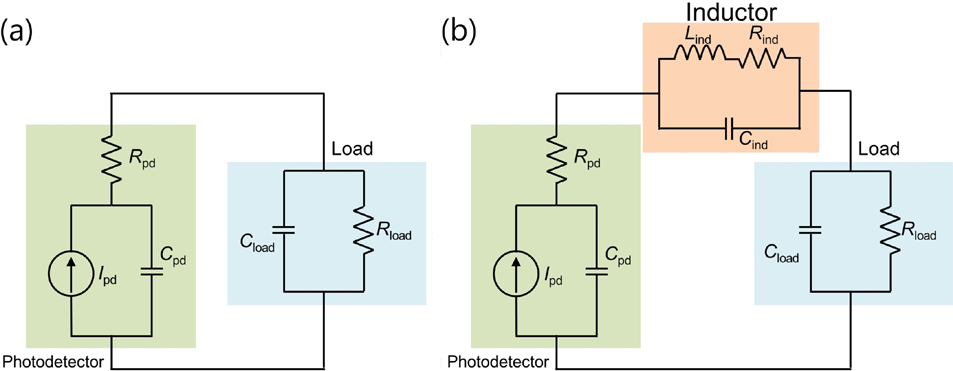
The basic principle is to introduce inductors into the photodetector. When the photodetector works at a high frequency, some capacitance effects of the photodetector can be offset by the introduced inductance. This leads to an increase in the frequency response curves at high frequencies, thereby increasing the bandwidth. The equivalent RC circuit of the Ge waveguide photodetector is replaced by the equivalent RLC circuits of the photodetector with integrated inductor. An equivalent RC circuit and RLC circuit of Ge waveguide photodetector are shown inFigs. 1(a) and1(b), respectively.

Figure 1.(Color online) Equivalent circuit of Ge waveguide photodetector (a) without and (b) with integrated inductor.
Device fabrication and inductive characteristics
The Ge waveguide photodetectors were fabricated on a silicon on insulator (SOI) substrate with a 220 nm-thick Si layer and a 2µm-thick buried oxide layer (BOX). As shown inFig. 2(a), the 220 nm-thick Si layer was etched to define the photodetector and Si waveguide. A 500 nm-thick Ge layer was selectively grown on p-type Si layer that was implanted with boron to form p-type Si contact layer. The Ge absorption area of photodetector was 5µm in width and 8µm in length. The top of Ge layer was implanted with phosphorous to form n-type Ge contact layer.
Figure 2.(Color online) (a) Cross section of the Ge waveguide photodetector. (b) Microscopic image of the device. (c) Microscopic image of the standalone inductors (L1, L2, L3, L4, and L5).
The first via and metal to n-type Ge/p-type Si were fabricated, followed by the second via and metal to form pads and various integrated inductors (L1, L2, L3, L4, and L5). The inductors were formed by a two-loop square spiral with 10µm width traces. The inner loops of inductors were 20, 30, 40, 50, and 60µm in side lengths, while the outer loops were 70, 80, 90, 100, and 110µm in side lengths, respectively. Finally, the pad contact holes were fabricated to connect test probes.Fig. 2(b) shows the microscopic image of the device with integrated inductor and pads.
Simultaneously, to determine the specific parameter values of integrated inductors, standalone spiral inductors with separate pads were also fabricated.Fig. 2(c) shows the microscopic image of standalone inductors (L1, L2, L3, L4, and L5). The structures of standalone inductors (L1, L2, L3, L4, and L5) are similar to those of integrated inductors. TheS-parameters of standalone inductors were measured using a vector network analyzer and a radio-frequency ground-signal (GS) probe. The upper frequency of GS probe is 40 GHz, and the test range is from 10 MHz to 10 GHz, which can represent the characteristics of standalone inductors. The parameters of inductors are extracted based on the equivalent circuit, as shown inFig. 3(a).Figs. 3(b)–3(f) show the fittingS-parameter curves of standalone inductors (L1, L2, L3, L4, and L5), respectively. The blue curves represent measured data while the red curves represent fitting results. The extracted inductance (Lind) of standalone inductors (L1, L2, L3, L4, and L5) are 240, 290, 350, 410, and 450 pH, with the resistances (Rind) \ capacitances (Cind) values of 2.5\7, 3.2\7, 4.0\8, 4.8\8, and 5.0\9 Ω\fF, respectively.
Figure 3.(Color online) (a) Equivalent circuit of the extracted parameters of inductors. (b–f) Fitting curves of the standalone inductors (L1, L2, L3, L4, and L5).
Results and discussion
The current–voltage (I–V) characteristics of Ge waveguide photodetectors with and without incident light are measured using an Agilent B1500A semiconductor parameter analyzer, a probe station and a Santec tunable semiconductor laser TSL-550 (1500–1630 nm) at room temperature. The incident light is introduced into the Si waveguide of photodetectors by a single-mode tapered fiber. The coupling loss between the tapered lensed fiber and Si waveguide is about –5.72 dB at an incident light wavelength of 1550 nm. The optical power output from the tapered lensed fiber is measured to be 0 dBm by a calibrated commercial reference detector. Accordingly, the incident optical power of photodetectors is about –5.72 dBm.Fig. 4(a) shows theI–V characteristics of the Ge waveguide photodetector in dark and with 1550 nm incident light.Fig. 4(b) shows dark currents of Ge waveguide photodetectors without and with integrated inductors (L1, L2, L3, L4, and L5) at a bias voltage from 1 to –3 V. Dark currents of these photodetectors are similar, revealing the consistency among photodetectors with various integrated inductors. As shown in the inset ofFig. 4(b), at –1 V bias voltage, the dark currents and 1550 nm optical responsivities of these photodetectors are approximately 35 nA and 0.81 A/W, respectively, showing little difference between photodetectors without and with different inductances. These results show that the inductor gain peaking technique does not substantially change the basic performance of Ge waveguide photodetector, including dark current and optical response characteristics.
Figure 4.(Color online) (a) Typical current–voltage characteristics of the Ge waveguide photodetector with and without incident light. (b) Dark current characteristics of Ge waveguide photodetectors without and with integrated inductors. Inset shows the dark current and responsivity of these photodetectors.
High-frequency characteristics of Ge waveguide photodetectors are measured using an Agilent 67 GHz lightwave component analyzer (LCA) N4373D in test ranges from 10 MHz to 67 GHz, and a radio-frequency ground-signal-ground (GSG) probe of 65 GHz with 50 Ω load resistances. The modulated output light at 1550 nm from the integrated Agilent LCA system is transmitted through optical fibers, and an optical polarizer is used to maximize the incident light power in photodetectors. The bias voltage from Keithley 2611A system source meter is applied to photodetectors through the integrated Agilent LCA system via GSG probe. The frequency responses between 50–75 GHz are measured using the optical heterodyne beat frequency system with a 75 GHz RF power meter. The photocurrent of devices is approximately 200µA. The normalized frequency responses of these photodetectors at 1550 nm are shown inFig. 5. The dotted lines represent measured normalized frequency responses of Ge waveguide photodetectors with and without integrated inductors, while the solid lines represent fitted results between 0–67 GHz and the measured frequency responses between 67–75 GHz. An evident inductive-gain-peaking effect can be observed here. The normalized output RF power of photodetectors with integrated inductors is improved at high frequency. The bandwidths gradually decrease as inductances of integrated inductors increase from L1 to L5. At a bias voltage of –3 V, bandwidths of photodetectors without and with integrated inductors (L1, L2, L3, L4, and L5) are 28, >75, 75, 68, 62, and 58 GHz, respectively. The 3-dB bandwidth up to 75 GHz is achieved at –3 V, which is one of the highest bandwidth values reported among inductive-gain-peaking photodetectors[18-22].
Table Infomation Is Not Enable
Figure 5.(Color online) Frequency responses of Ge waveguide photodetectors with and without integrated inductors.
Table Infomation Is Not Enable
Additionally, bandwidth of the photodetector with integrated inductor strongly depends on the peak values of normalized output RF power. As shown inFig. 5, the peak positions of normalized frequency responses of the photodetectors with integrated inductors (L1, L2, L3, L4, and L5) are 67, 60, 54, 48, and 43 GHz, respectively. The peak values increase with the increase in inductance. This is attributed to the inductive-gain-peaking effect[18].
To investigate the relationship between bandwidth with parameters of integrated inductors, the frequency responses of photodetectors without and with integrated inductors are simulated based on equivalent RC/RLC circuits. Parameters of the equivalent RC/RLC circuits used in simulation are displayed inTable 1. The series resistance (Rpd) extracted from forwardI–V characteristics is about 110 Ω[23]. The junction capacitance is written asCj =εε0WL/d, whereε andε0 are the relative and vacuum permittivity, respectively;W andL are the width and length of the photodetectors, respectively, andd is the thickness of intrinsic layer. The junction capacitanceCj is about 15.25 fF for a detector withd = 400 nm,W = 5µm, andL = 8µm. The load resistanceRload is 50 Ω and load capacitanceCp is 17 fF. The inductance (Lind), resistance (Rind), and capacitance (Cind) of integrated inductors (L1, L2, L3, L4, and L5) are extracted from theS-parameters of inductors inFig. 3.Fig. 6(a) shows the simulated frequency response of photodetectors without and with integrated inductors. The simulated 3-dB bandwidths of photodetectors without and with integrated inductors (L1, L2, L3, L4, and L5) are 29, 80, 75, 67, 61, and 58 GHz, respectively.
Figure 6.(Color online) (a) Simulated frequency response of the photodetector without and with integrated inductors. (b) Simulated 3-dB bandwidth and peak values.
The simulated 3-dB bandwidths are extracted based on multiple sets of parameters of inductors.Fig. 6(b) shows the 3-dB bandwidths and peak values of normalized RF power of photodetectors with integrated inductors. The blue and red lines represent the simulated bandwidths and peak values of the normalized RF power, respectively. The solid green dots represent experimental results. The simulated bandwidths of photodetectors with integrated inductors (L1, L2, L3, L4, and L5) are in agreement with the values achieved via experimental results. The 3-dB bandwidths of photodetectors initially increase and subsequently decrease as the inductance (Lind) of inductors increases. WhenLind is about 170 pH, the 3-dB bandwidth is maximum. WhenLind > 170 pH, the bandwidth gradually decreases. WhenLind < 260 pH, there is no RF power peak in the frequency response curve. WhenLind > 260 pH, the peak RF power gradually increases as the inductance (Lind) increases. Therefore, to ensure a larger bandwidth and a high peak value, the integrated inductor can be neither too large nor too small. A suitably large inductance is required to ensure that the frequency response curve does not decrease to –3 dB before the inductive gain peak, and to ensure the occurrence of the inductive gain peak in the frequency response curve. Simultaneously, a slightly smaller inductance is required to extend to a larger bandwidth.
To investigate the data transmission characteristics of Ge waveguide photodetectors with integrated inductors in high-speed communication systems, eye diagrams of these photodetectors are measured on wafer. A (231−1) long optical nonreturn-to-zero (NRZ) pseudorandom bit sequence data pattern with various Gbps data rates generated by a commercial LiNbO3 electro-optical Mach-Zehnder intensity modulator is delivered to the waveguide of these photodetectors. The upper limit of the LiNbO3 modulator is 65 Gbps. The eye diagrams of photodetectors without and with integrated inductors at 50, 55, 60, and 64 Gbps data rates are presented inFig. 7. The photocurrent of the devices is approximately 300µA. The integration time of eye diagram is approximately 40 s. At 50, 55, 60, and 64 Gbps data transfer rates, all eye diagrams open clearly. These results prove that Ge waveguide photodetectors with integrated inductors exhibit good data transmission characteristics. Additionally, as the inductance of integrated inductors increases from 240 pH (L1) to 450 pH (L5), the eye diagram becomes clearer. This phenomenon could be attributed to the increased output RF power with the increasing inductance at 20–40 GHz, which covers the fundamental frequencies of the signals at 50–64 Gbps.
Figure 7.(Color online) Eye diagrams of Ge waveguide photodetectors with and without integrated inductors at 50, 55, 60, and 64 Gbps.
Fig. 8 shows the measured signal-to-noise ratios (SNR) and the eye amplitude of the eye diagrams. At 50 and 64 Gbps data rates, the overall value of the SNR increases as the inductance of integrated inductors rises from L1 to L5. The SNR of the eye diagram has been established to be related to noise and photocurrent intensity[23]. The SNR of some data points is low because its photocurrent is slightly lower during the measurement, which can be obtained from the eye amplitude. This also shows that the data receiving capability of the integrated inductive photodetectors with the largest bandwidth which is not necessarily the best. When the inductive-gain-peaking technique is used in actual device production, the relationship between the frequency response and data processing capability should be weighed, to select the optimal integrated inductor to improve the speed of a typical Ge waveguide photodetector.Table 2 shows the performance summary of high-speed silicon-based Ge photodetectors with integrated inductances. As can be seen inTable 2, our fabricated photodetector with inductance has a high measured bandwidth, which is one of the highest bandwidth values among inductive-gain-peaking photodetectors.
Figure 8.(Color online) Measured signal-to-noise ratio (SNR) and eye amplitude of the eye diagram at 50 and 64 Gbps.
Conclusion
To summarize, high speed Ge waveguide photodetectors with integrated inductors (L1, L2, L3, L4, and L5) are designed and fabricated using the inductive-gain-peaking technique. The inductive-gain-peaking technique does not substantially change the dark current and responsivity characteristics. At –1 V bias voltage, dark currents and 1550 nm optical responsivities of these photodetectors are approximately 35 nA and 0.81 A/W, respectively. The inductance of integrated inductors affects the peak value of the normalized output RF power and determines the 3-dB bandwidth. The peak value of the normalized output RF power gradually increases when the inductance of the integrated inductor increases from 240 pH (L1) to 450 pH (L5). The 3-dB bandwidths of the photodetectors with integrated inductors (L1, L2, L3, L4, and L5) are >75, 75, 66, 60 and 58 GHz, respectively. The corresponding inductance of the integrated inductors (L1, L2, L3, L4, and L5) are 242, 280, 360, 415, and 460 pH, respectively. Within a certain range, the smaller the inductance of the integrated inductor, the larger the 3-dB bandwidth obtained. However, the appropriate inductance should be selected to ensure a high output RF power. The eye diagrams open more clearly from the integrated inductors (L1) to the integrated inductors (L5) due to the increased output RF power with the increasing inductance at 20–40 GHz, which covers the fundamental frequencies of the signals at 50–64 Gbps. When the inductive-gain-peaking technique is used to improve the speed of a typical photodetector, the relationship between the frequency response and data processing capability should be weighed to select an optimal integrated inductor.
References
[1] D Marpaung, J P Yao, J Capmany. Integrated microwave photonics. Nat Photonics, 13, 80(2019).
[2] D Zhou, C L Sun, Y X Lai et al. Integrated silicon multifunctional mode-division multiplexing system. Opt Express, 27, 10798(2019).
[3] Y C Shi, Y Zhang, Y T Wan et al. Silicon photonics for high-capacity data communications. Photonics Res, 10, A106(2022).
[4] Y Salamin, P Ma, B Baeuerle et al. 100 GHz plasmonic photodetector. ACS Photonics, 5, 3291(2018).
[5] Z Liu, F Yang, W Z Wu et al. 48 GHz high-performance Ge-on-SOI photodetector with zero-bias 40 Gbps grown by selective epitaxial growth. J Lightwave Technol, 35, 5306(2017).
[6] L Vivien, D Marris-Morini, J-M Fédéli et al. Metal-semiconductor-metal Ge photodetectors integrated in silicon waveguides. Appl Phy Lett, 92, 151114(2008).
[7] C T DeRose, D C Trotter, W A Zortman et al. Ultra compact 45 GHz CMOS compatible Germanium waveguide photodiode with low dark current. Opt Express, 19, 24897(2011).
[8] Y P Zhu, Z Liu, C Q Niu et al. High-speed and high-power germanium photodetector based on a trapezoidal absorber. Opt Lett, 47, 3263(2022).
[9] M Cea, D Orden, J Fini et al. High-speed, zero-biased silicon-germanium photodetector. APL Photonics, 6, 041302(2021).
[10] H Chen, P Verheyen, P De Heyn et al. –1 V bias 67 GHz bandwidth Si-contacted germanium waveguide p-i-n photodetector for optical links at 56 Gbps and beyond. Opt Express, 24, 4622(2016).
[11] S Lischke, D Knoll, C Mai et al. High bandwidth, high responsivity waveguide-coupled germanium p-i-n photodiode. Opt Express, 23, 27213(2015).
[12] R Going, T J Seok, J Loo et al. Germanium wrap-around photodetectors on silicon photonics. Opt Express, 23, 11975(2015).
[13] S Lischke, A Peczek, J S Morgan et al. Ultra-fast germanium photodiode with 3-dB bandwidth of 265 GHz. Nat Photonics, 15, 925(2021).
[14] X Hu, D Y Wu, H G Zhang et al. High-speed and high-power germanium photodetector with a lateral silicon nitride waveguide. Photonics Res, 9, 749(2021).
[15] T Yin, R Cohen, M M Morse et al. 31 GHz Ge n-i-p waveguide photodetectors on silicon-on-insulator substrate. Opt Express, 15, 13965(2007).
[16] S R Liao, N N Feng, D Z Feng et al. 36 GHz submicron silicon waveguide germanium photodetector. Opt Express, 19, 10967(2011).
[17] L Vivien, J Osmond, J M Fédéli et al. 42 GHz p. i. n germanium photodetector integrated in a silicon-on-insulator waveguide. Opt Express, 17, 6252(2009).
[18] M Gould, T Baehr-Jones, R Ding et al. Bandwidth enhancement of waveguide-coupled photodetectors with inductive gain peaking. Opt Express, 20, 7101(2012).
[19] A Novack, M Gould, Y S Yang et al. Germanium photodetector with 60 GHz bandwidth using inductive gain peaking. Opt Express, 21, 28387(2013).
[20] D Y Wu, X Hu, W Z Li et al. 62 GHz germanium photodetector with inductive gain peaking electrode for photonic receiving beyond 100 Gbaud. J Semicond, 42, 020502(2021).
[21] Y Shi, D Zhou, Y Yu et al. 80 GHz germanium waveguide photodiode enabled by parasitic parameter engineering. Photonics Res, 9, 605(2021).
[22] G Y Chen, Y Yu, S P Deng et al. Bandwidth improvement for germanium photodetector using wire bonding technology. Opt Express, 23, 25700(2015).
[24] W Z Li, H G Zhang, X Hu et al. 100 Gbit/s co-designed optical receiver with hybrid integration. Opt Express, 29, 14304(2021).