• Photonics Research
  • Vol. 6, Issue 5, B1 (2018)
Andres D. Neira, Gregory A. Wurtz*, and Anatoly V. Zayats
Author Affiliations
  • Department of Physics, King’s College London, Strand, London WC2R 2LS, UK
  • show less
    DOI: 10.1364/PRJ.6.0000B1 Cite this Article Set citation alerts
    Andres D. Neira, Gregory A. Wurtz, Anatoly V. Zayats. All-optical switching in silicon photonic waveguides with an epsilon-near-zero resonant cavity [Invited][J]. Photonics Research, 2018, 6(5): B1 Copy Citation Text show less
    (a) Schematic of the modulator composed of two layers of ENZ metamaterial integrated in a conventional Si waveguide and separated by a gap. (b) Design based on plasmonic nanorods. The frequency to achieve the ENZ condition can be tuned by varying the diameter of and separation between nanorods.
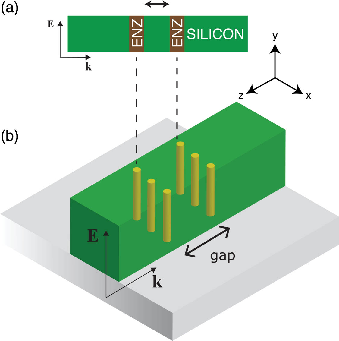
    Fig. 1. (a) Schematic of the modulator composed of two layers of ENZ metamaterial integrated in a conventional Si waveguide and separated by a gap. (b) Design based on plasmonic nanorods. The frequency to achieve the ENZ condition can be tuned by varying the diameter of and separation between nanorods.
    Transmission of the cavity for different nanorod diameters and gaps. (a) TMM calculations. In this geometry, schematically shown in Fig. 1(a), the nanorod metamaterial layers are replaced by homogenenized layers of thickness corresponding to one unit cell of the nanostructured metamaterial. (b) Dependence of the effective permittivity of the metamaterial layer on the nanorod diameter. (c) Full-vectorial 3D simulation of the transmission of the waveguide-integrated modulator for different nanorod diameters and gaps. (d) Intensity distribution of the guided mode for (left) low- and (right) high-transmission states occuring for the gaps of ∼100 nm and ∼180 nm, respectively. The nanorod diameter was set to 35 nm with the distance between nanorods being 90 nm; the waveguide cross-sectional dimension is 340 nm×300 nm. All simulations were performed at a wavelength of 1.55 μm.
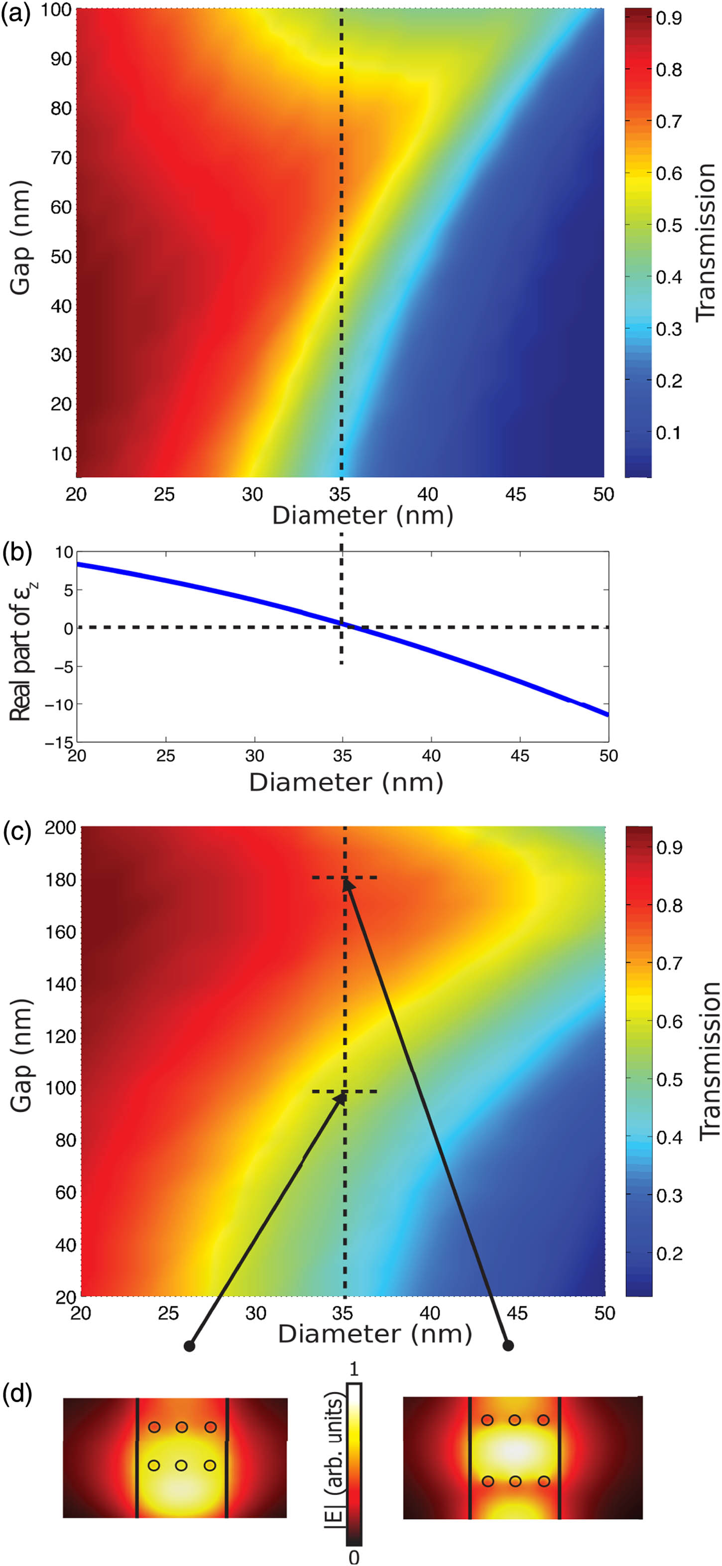
    Fig. 2. Transmission of the cavity for different nanorod diameters and gaps. (a) TMM calculations. In this geometry, schematically shown in Fig. 1(a), the nanorod metamaterial layers are replaced by homogenenized layers of thickness corresponding to one unit cell of the nanostructured metamaterial. (b) Dependence of the effective permittivity of the metamaterial layer on the nanorod diameter. (c) Full-vectorial 3D simulation of the transmission of the waveguide-integrated modulator for different nanorod diameters and gaps. (d) Intensity distribution of the guided mode for (left) low- and (right) high-transmission states occuring for the gaps of 100  nm and 180  nm, respectively. The nanorod diameter was set to 35 nm with the distance between nanorods being 90 nm; the waveguide cross-sectional dimension is 340  nm×300  nm. All simulations were performed at a wavelength of 1.55 μm.
    Transmission spectra of the modulator in ON and OFF states and the modulation depth obtained from full-vectorial simulations for the resonance conditions shown in Fig. 2(b): nanorods with 35 nm diameter, 90 nm period, and 180 nm gap. Insets show the guided mode intensity distributions along the waveguide modulator at different wavelengths (1.1, 1.3, and 1.55 μm) and transmission states for the mode propagating from the bottom to the top of the waveguide.
    Fig. 3. Transmission spectra of the modulator in ON and OFF states and the modulation depth obtained from full-vectorial simulations for the resonance conditions shown in Fig. 2(b): nanorods with 35 nm diameter, 90 nm period, and 180 nm gap. Insets show the guided mode intensity distributions along the waveguide modulator at different wavelengths (1.1, 1.3, and 1.55 μm) and transmission states for the mode propagating from the bottom to the top of the waveguide.
    Andres D. Neira, Gregory A. Wurtz, Anatoly V. Zayats. All-optical switching in silicon photonic waveguides with an epsilon-near-zero resonant cavity [Invited][J]. Photonics Research, 2018, 6(5): B1
    Download Citation