Andres D. Neira, Gregory A. Wurtz*, and Anatoly V. Zayats
Abstract
Strong nonlinearity of plasmonic metamaterials can be designed near their effective plasma frequency in the epsilon-near-zero (ENZ) regime. We explore the realization of an all-optical modulator based on the Au nonlinearity using an ENZ cavity formed by a few Au nanorods inside a Si photonic waveguide. The resulting modulator has robust performance with a modulation depth of about 30 dB/μm and loss less than 0.8 dB for switching energies below 600 fJ. The modulator provides a double advantage of high mode transmission and strong nonlinearity enhancement in the few-nanorod-based design.1. INTRODUCTION
Photonic integrated circuits (PICs) provide passive and active functionalities to control the flow of optical signals, such as spectral filters, optical multiplexers, electro-optical modulators, photodetectors, and interferometers [1–6]. Silicon photonics has proven to be an excellent platform for photonic integration as silicon has a high refractive index () and low optical losses at telecom wavelengths, while its nanofabrication is compatible with CMOS industry standards, allowing for direct compatibility with electronics [7–10]. Several electro-optical modulators have been demonstrated on a Si platform using resonant structures such as Mach–Zehnder interferometers [9,10], waveguide-ring-resonator geometries [7], and a hybrid Si-plasmonic platform [11,12] based on the application of an electric field via electrical interconnections, thus limiting the maximum modulation speed to a few tens of gigahertz.
All-optical modulation overcomes this barrier since it relies on ultrafast nonlinear optical processes such as two-photon absorption, free carrier heating, or the Franz–Keldysh effect, achieving modulation speeds exceeding 100 Gbit/s [3–5,12–16]. Nevertheless, nonlinear optical processes are generally weak requiring a high energy per bit to be practically observable. Recently, surface plasmon excitations in metallic structures have been used to reduce the energy requirement of nonlinear optical processes, since the electric field is enhanced in plasmonic nanostructures at sub-wavelength scales, allowing efficient light–matter interactions [17]. Several approaches have already demonstrated the use of such an enhancement to achieve nonlinear switching in various geometries including plasmonic waveguides, particles, and nano-antennas, as well as metamaterials [18–22]. In particular, hyperbolic plasmonic metamaterials [23] have been shown to provide high-speed and low-energy all-optical modulation in both free-space and integrated geometries [24–28] owing to strong nonlinearity and high sensitivity to refractive index changes. The metamaterial waveguides also provide important opportunities for guided mode dispersion engineering [28–31].
In hyperbolic metamaterials, the nonlinearity is particularly enhanced in the so-called -near-zero (ENZ) regime near the effective plasma frequency [27], where one component of the effective permittivity tensor of the metamaterial is vanishingly small []. Not only is the nonlinear optical response of the metamaterial in this regime strong, but it can also be tuned through the metamaterial’s geometrical design to the required operating wavelength [25,32].
Sign up for Photonics Research TOC. Get the latest issue of Photonics Research delivered right to you!Sign up now
In this context, all-optical modulators using the concept of hyperbolic metamaterials based on plasmonic nanorods integrated with silicon photonics have been proposed [26]. In order to further reduce losses associated with the use of metals and subsequently reduce switching energy requirements and modulation efficiency, the reduction of the number of metallic meta-atoms [33] in a metamaterial modulator is desirable. This, however, needs to be achieved while preserving the conditions required for efficient modulation.
In this paper, we explore the realization of an all-optical modulator using an optically switchable cavity based on the nonlinearity of Au nanorods embedded in a Si waveguide and forming a metamaterial operating in the ENZ regime. Using full-vectorial electromagnetic simulations, it is shown that the effective medium theory (EMT), used for the description of the average optical properties of the metamaterial, is still applicable for the description of the optical response of the ENZ layers made of a metamaterial formed by only a few nanorods. Metamaterial behavior has indeed been recently experimentally observed with only a few meta-atoms in the structure [30]. The designed integrated modulator has strong nonlinear behavior with a switching energy of about 600 fJ for a modulation contrast of about 30% in a device showing an insertion loss of about 0.96 dB.
2. RESULTS AND DISCUSSION
Figure 1(a) shows the schematics of the design of the switchable ENZ cavity implemented in the Si waveguide. The ENZ layers provide high reflectivity, resulting in a resonant cavity that allows the resonant transmission of light at a wavelength dependent on the cavity length. The two hyperbolic mirrors are integrated in a single-mode silicon waveguide with a cross section of 340 nm in height and 300 nm in width, and thus supporting a fundamental TM-like polarized mode at a telecom wavelength of 1.55 μm. The cavity’s length is designed for the resonant transmission of this mode at the operating wavelength. For the mode considered in this study, the component of the permittivity tensor of the metamaterial forming the ENZ layers can be modeled in a good approximation using the effective medium theory as , where and represent the permittivity of silicon ( at 1.55 μm) and Au, respectively, and is the nanorod concentration as calculated in a uniform medium with a nanorod interdistance and nanorod diameter 2a [34].
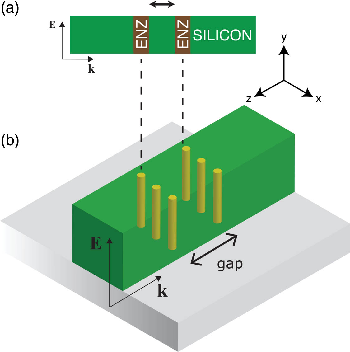
Figure 1.(a) Schematic of the modulator composed of two layers of ENZ metamaterial integrated in a conventional Si waveguide and separated by a gap. (b) Design based on plasmonic nanorods. The frequency to achieve the ENZ condition can be tuned by varying the diameter of and separation between nanorods.
The cavity length between the ENZ layers needed to achieve the resonant transmission of the TM mode is found by simulating the waveguide transmission for different geometrical parameters of the cavity at the chosen telecom wavelength. In the first approximation, the transmission of the TM mode through the multilayer system shown in Fig. 1(a) is simulated using the transfer matrix method (TMM) [26]. Since the variation of either nanorod separation in the direction or radius is equivalent to a variation in the nanorod concentration, we fixed the value and evaluated the dependence of the transmission varying the cavity length and the diameter of the nanorod [Fig. 2(a)]. If the distance between the nanorods in the direction perpendicular to the waveguide direction and the gap have different values, the overall metamaterial inclusion can also be considered as anisotropic in the -plane.

Figure 2.Transmission of the cavity for different nanorod diameters and gaps. (a) TMM calculations. In this geometry, schematically shown in Fig. 1(a), the nanorod metamaterial layers are replaced by homogenenized layers of thickness corresponding to one unit cell of the nanostructured metamaterial. (b) Dependence of the effective permittivity of the metamaterial layer on the nanorod diameter. (c) Full-vectorial 3D simulation of the transmission of the waveguide-integrated modulator for different nanorod diameters and gaps. (d) Intensity distribution of the guided mode for (left) low- and (right) high-transmission states occuring for the gaps of and , respectively. The nanorod diameter was set to 35 nm with the distance between nanorods being 90 nm; the waveguide cross-sectional dimension is . All simulations were performed at a wavelength of 1.55 μm.
The ENZ condition of the homogenized metamaterial for a diameter of 35 nm [Fig. 2(b)] separates two regimes of transmission [Fig. 2(a)]. The transmission is high for nanorod diameters smaller 35 nm (elliptic dispersion) but significantly suppressed for nanorods with larger diameters (hyperbolic dispersion). This can be understood considering the nanorod concentration . A relatively low concentration corresponds to the former regime with an effective permittivity close to that of silicon, and thus the TM mode propagates as if the metamaterial was absent.
As the nanorod concentration increases and the effective permittivity approaches that of the metal, the metamaterial becomes more reflective, allowing the resonant transmission of the TM mode at a given gap value, in the considered case around 80 nm [Fig. 2(a)]. The same is true regarding losses, which are related to the imaginary part of the effective permittivity. The losses due to the presence of metal will also increase with increasing concentration, so that only close to the ENZ regime is it possible to obtain resonant behavior of the cavity without a substantial drop in the transmission [Fig. 2(a)]. Thus, the best characteristics of the cavity with high reflectivity and high resonant transmission can be achieved when the metamaterial operates in the ENZ regime.
To reduce absorption and insertion loss, the considered metamaterial is composed of only a few nanorods [Fig. 1(b)]. Therefore, it is instructive to compare the applicability of the EMT approach with full-vectorial numerical simulations [35] taking into account the microscopic structure of the modulator [Fig. 2(c)]. Interestingly, the EMT and microscopic simulations have similar parametric dependence despite being applied to only one layer of nanorods. The transition between the two regimes of high and low transmissions is dictated by the ENZ condition. The analysis of the mode intensity distributions shows that in the high-transmission state, the cavity mode is built up between two layers of nanorods, and the transmission is high. In the low-transmission state, the mode is mainly reflected. Due to the small number of Au nanorods involved, the dissipative loss is minimal with about 20% of the mode absorbed, and the cavity -factor reaches a value of 3 even for this low nanorod concentration.
The resonant value of the cavity gap obtained using 3D numerical analysis is about 180 nm [Fig. 2(c)], measured between the nanorod axis. (The actual Si thickness measured between effective metamaterial layer edges is 90 nm, which is close to the value of 80 nm obtained using the effective medium theory above.) The similarity of both the values found and the behavior observed allows us to conclude that the effective medium theory can still accurately model the optical behavior of metamaterials composed of only a few nanorods, which was also confirmed by the experimental measurements of hyperbolic crystals based on plasmonic nanorods [30].
In order to realize all-optical modulation with the integrated metamaterial-based cavity in a Si waveguide, we make use of the dynamic tuneability of the ENZ frequency condition, which can be achieved using the nonlinear response of Au [24–27]. The nonlinear optical properties of the metamaterial are modeled considering the nonlinearity of free electrons in Au using the random phase approximation together with the two-temperature model accounting for the dependence of electron scattering on both electron and lattice temperatures [18,25,36]. In the infrared wavelength range, the predominant contribution to the Au polarizability comes from intraband transitions, and, therefore, its permittivity can be reduced to a Drude-like contribution: where is the Au plasma frequency, is the electron scattering rate, including both electron–electron and electron–phonon scattering as a function of the temperature of electrons () and lattice (), respectively, and is the high-frequency limit of the permittivity [18]. The electron temperature is determined by the equilibrium Fermi–Dirac distribution and modified by the absorption of photons from a control beam, while the lattice temperature is assumed constant, which represents a satisfactory approximation for the (sub-)picosecond timescales of interest in this study [16,25]. Temperature effects in Si were neglected for the control light energies and timescales considered.
The switching of the modulator is determined by a control pulse ( duration), which upon absorption by the metamaterial changes the electron temperature in the nanorods, resulting in changes of the permittivity of Au [Eq. (1)]. This, in turn, influences the optical properties of the metamaterial and the cavity transmission. The latter process was simulated assuming the ON (low-transmission) and OFF (high-transmission) state electron temperatures and , which correspond to typical temperature modifications in nonlinear femtosecond experiments with Au and Au-based metamaterials [16,24,27]. Strong, up to 30%, changes in the modulator transmission have been observed (Fig. 3). In the ON state, the decreased transmission is mainly due to increased ohmic losses. This is seen in Fig. 3 from the intensity variations along the waveguide for the ON state. In the ENZ regime the absolute value of the permittivity is close to zero and, therefore, is very sensitive to any variation in the imaginary part of the permittivity, influencing the -factor of the cavity.
Figure 3.Transmission spectra of the modulator in ON and OFF states and the modulation depth obtained from full-vectorial simulations for the resonance conditions shown in Fig. 2(b): nanorods with 35 nm diameter, 90 nm period, and 180 nm gap. Insets show the guided mode intensity distributions along the waveguide modulator at different wavelengths (1.1, 1.3, and 1.55 μm) and transmission states for the mode propagating from the bottom to the top of the waveguide.
The performance of the ENZ cavity as an all-optical modulator can be characterized in terms of both the total absorbed energy needed to achieve the ON state from the OFF state and the modulator’s insertion losses. The first can be calculated assuming a uniform electron temperature across the nanorods [25,27]: where is the heat capacity of electrons () and is the total volume of the nanorods. For the modulator considered, a total energy of 600 fJ is required to achieve the increase of the electron temperature needed for the 30% transmission modulation demonstrated above. Additionally, the insertion losses evaluated for this geometry are and the extinction of about . This high value is a consequence of the strong field confinement in the cavity, allowing a strong modulation with a very small modulator size and low switching energy.
3. CONCLUSION
An all-optical modulator has been proposed, based on ultrathin metamaterial mirrors made of a few Au nanorods, forming an ENZ cavity inside a Si waveguide. The strong nonlinear optical response of the optimized ENZ cavity allows all-optical switching and enables integrated nanoscale switches and modulators in Si waveguides. A similar approach can be used for integrated thermo-optical modulators [37] using the control of the lattice temperature of metal.
Acknowledgment
Acknowledgment. Anatoly V. Zayats acknowledges support from the Royal Society and the Wolfson Foundation. Gregory A. Wurtz acknowledges support from the EC. The data access statement: all data supporting this research are provided in full in the results section.
References
[1] D. A. B. Miller. Device requirements for optical interconnects to silicon chips. Proc. IEEE, 97, 1166-1185(2009).
[2] A. V. Krasavin, A. V. Zayats. Active nanophotonic circuitry based on dielectric-loaded plasmonic waveguides. Adv. Opt. Mater., 3, 1662-1690(2015).
[3] C. Koos, P. Vorreau, T. Vallaitis, P. Dumon, W. Bogaerts, R. Baets, B. Esembeson, I. Biaggio, T. Michinobu, F. Diederich, W. Freude, J. Leuthold. All-optical high-speed signal processing with silicon-organic hybrid slot waveguides. Nat. Photonics, 3, 216-219(2009).
[4] M. Hochberg, T. Baehr-Jones, G. Wang, M. Shearn, K. Harvard, J. Luo, B. Chen, Z. Shi, R. Lawson, P. Sullivan, A. K. Y. Jen, L. Dalton, A. Scherer. Terahertz all-optical modulation in a silicon-polymer hybrid system. Nat. Mater., 5, 703-709(2006).
[5] D. J. Moss, R. Morandotti, A. L. Gaeta, M. Lipson. New CMOS-compatible platforms based on silicon nitride and Hydex for nonlinear optics. Nat. Photonics, 7, 597-607(2013).
[6] C. P. T. McPolin, J.-S. Bouillard, S. Vilain, A. V. Krasavin, W. Dickson, D. O’Connor, G. A. Wurtz, J. Justice, B. Corbett, A. V. Zayats. Integrated plasmonic circuitry on a vertical-cavity surface-emitting semiconductor laser platform. Nat. Commun., 7, 12409(2016).
[7] Q. Xu, B. Schmidt, S. Pradhan, M. Lipson. Micrometre-scale silicon electro-optic modulator. Nature, 435, 325-327(2005).
[8] H. Subbaraman, X. Xu, A. Hosseini, X. Zhang, Y. Zhang, D. Kwong, R. T. Chen. Recent advances in silicon-based passive and active optical interconnects. Opt. Express, 23, 2487-2511(2015).
[9] C. Sun, M. T. Wade, Y. Lee, J. S. Orcutt, L. Alloatti, M. S. Georgas, A. S. Waterman, J. M. Shainline, R. R. Avizienis, S. Lin, B. R. Moss, R. Kumar, F. Pavanello, A. H. Atabaki, H. M. Cook, A. J. Ou, J. C. Leu, Y.-H. Chen, K. Asanović, R. J. Ram, M. A. Popović, V. M. Stojanović. Single-chip microprocessor that communicates directly using light. Nature, 528, 534-538(2015).
[10] A. Novack, M. Streshinsky, R. Ding, Y. Liu, A. E.-J. Lim, G.-Q. Lo, T. Baehr-Jones, M. Hochberg. Progress in silicon platforms for integrated optics. Nanophotonics, 3, 205-214(2014).
[11] K. Liu, C. R. Ye, S. Khan, V. J. Sorger. Review and perspective on ultrafast wavelength-size electro-optic modulators. Laser Photon. Rev., 9, 172-194(2015).
[12] V. E. Babicheva, N. Kinsey, G. V. Naik, M. Ferrera, A. V. Lavrinenko, V. M. Shalaev, A. Boltasseva. Towards CMOS-compatible nanophotonics: ultra-compact modulators using alternative plasmonic materials. Opt. Express, 21, 27326-27337(2013).
[13] S. G. Carter, V. Birkedal, C. S. Wang, L. A. Coldren, A. V. Maslov, D. S. Citrin, M. S. Sherwin. Quantum coherence in an optical modulator. Science, 310, 651-653(2005).
[14] M. R. Shcherbakov, P. P. Vabishchevich, A. S. Shorokhov, K. E. Chong, D.-Y. Choi, I. Staude, A. E. Miroshnichenko, D. N. Neshev, A. A. Fedyanin, Y. S. Kivshar. Ultrafast all-optical switching with magnetic resonances in nonlinear dielectric nanostructures. Nano Lett., 15, 6985-6990(2015).
[15] S. Kodama, T. Yoshimatsu, H. Ito. 500 Gbit/s optical gate monolithically integrating photodiode and electroabsorption modulator. Electron. Lett., 40, 555-556(2004).
[16] L. Nicholls, F. J. Rodríguez-Fortuño, M. E. Nasir, R. M. Cordova-Castro, N. Olivier, G. A. Wurtz, A. V. Zayats. Ultrafast synthesis and switching of light polarization in nonlinear anisotropic metamaterials. Nat. Photonics, 11, 628-633(2017).
[17] M. Kauranen, A. V. Zayats. Nonlinear plasmonics. Nat. Photonics, 6, 737-748(2012).
[18] J. Y. Bigot, J. Y. Merle, O. Cregut, A. Daunois. Electron dynamics in copper metallic nanoparticles probed with femtosecond optical pulses. Phys. Rev. Lett., 75, 4702-4705(1995).
[19] A. E. Nikolaenko, F. De Angelis, S. A. Boden, N. Papasimakis, P. Ashburn, E. Di Fabrizio, N. I. Zheludev. Carbon nanotubes in a photonic metamaterial. Phys. Rev. Lett., 104, 153902(2010).
[20] M. Ren, B. Jia, J.-Y. Ou, E. Plum, J. Zhang, K. F. MacDonald, A. E. Nikolaenko, J. Xu, M. Gu, N. I. Zheludev. Nanostructured plasmonic medium for terahertz bandwidth all-optical switching. Adv. Mater., 23, 5540-5544(2011).
[21] A. V. Krasavin, A. V. Zayats. Benchmarking system-level performance of passive and active plasmonic components: integrated circuits approach. Proc. IEEE, 104, 2338-2348(2016).
[22] C. McPolin, N. Olivier, J.-S. Bouillard, D. O’Connor, A. V. Krasavin, W. Dickson, G. A. Wurtz, A. V. Zayats. Universal switching of plasmonic signals using optical resonator modes. Light Sci. Appl., 6, e16237(2017).
[23] A. Poddubny, I. Iorsh, P. Belov, Y. Kivshar. Hyperbolic metamaterials. Nat. Photonics, 7, 948-957(2013).
[24] G. A. Wurtz, R. Pollard, W. Hendren, G. P. Wiederrecht, D. J. Gosztola, V. A. Podolskiy, A. V. Zayats. Designed ultrafast optical nonlinearity in a plasmonic nanorod metamaterial enhanced by nonlocality. Nat. Nanotechnol., 6, 107-111(2011).
[25] S. Peruch, A. Neira, G. A. Wurtz, B. Wells, V. A. Podolskiy, A. V. Zayats. Geometry defines ultrafast hot carrier dynamics and Kerr nonlinearity in plasmonic metamaterial waveguides and cavities. Adv. Opt. Mater., 5, 1700299(2017).
[26] A. D. Neira, G. A. Wurtz, P. Ginzburg, A. V. Zayats. Ultrafast all-optical modulation with hyperbolic metamaterial integrated in Si photonic circuitry. Opt. Express, 22, 10987-10994(2014).
[27] A. Neira, N. Olivier, M. Nasir, W. Dickson, G. A. Wurtz, A. V. Zayats. Eliminating material constraints for nonlinearity with plasmonic metamaterials. Nat. Commun., 6, 7757(2015).
[28] C. L. Cortes, Z. Jacob. Photonic analog of a van Hove singularity in metamaterials. Phys. Rev. B, 88, 045407(2013).
[29] N. Vasilantonakis, M. E. Nasir, W. Dickson, G. A. Wurtz, A. V. Zayats. Bulk plasmon-polaritons in hyperbolic nanorod metamaterial waveguides. Laser Photon. Rev., 9, 345-353(2015).
[30] W. Dickson, S. Beckett, C. McClatchey, A. Murphy, D. O’Connor, G. A. Wurtz, R. Pollard, A. V. Zayats. Hyperbolic polaritonic crystals based on nanostructured nanorod metamaterials. Adv. Mater., 27, 5974-5980(2015).
[31] A. D. Neira, G. A. Wurtz, A. V. Zayats. Superluminal and stopped light due to mode coupling in confined hyperbolic metamaterial waveguides. Sci. Rep., 5, 17678(2015).
[32] M. E. Nasir, S. Peruch, N. Vasilantonakis, W. P. Wardley, W. Dickson, G. A. Wurtz, A. V. Zayats. Tuning the effective plasma frequency of nanorod metamaterials from visible to telecom wavelengths. Appl. Phys. Lett., 107, 121110(2015).
[33] K. V. Sreekanth, A. De Luca, G. Strangi. Experimental demonstration of surface and bulk plasmon polaritons in hypergratings. Sci. Rep., 3, 3291(2013).
[34] J. Elser, R. Wangberg, V. A. Podolskiy, E. E. Narimanov. Nanowire metamaterials with extreme optical anisotropy. Appl. Phys. Lett., 89, 261102(2006).
[35] . Comsol Multiphysics 4.3a(2014).
[36] L. Jiang, H.-L. Tsai. Improved two-temperature model and its application in ultrashort laser heating of metal films. J. Heat Transfer, 127, 1167-1173(2005).
[37] S. Papaioannou, D. Kalavrouziotis, K. Vyrsokinos, J.-C. Weeber, K. Hassan, L. Markey, A. Dereux, A. Kumar, S. I. Bozhevolnyi, M. Baus, T. Tekin, D. Apostolopoulos, H. Avramopoulos, N. Pleros. Active plasmonics in WDM traffic switching applications. Sci. Rep., 2, 652(2012).


