• Photonics Research
  • Vol. 7, Issue 2, 121 (2019)
Anjin Liu1、2、3、*, Philip Wolf4, James A. Lott4, and Dieter Bimberg4、5
Author Affiliations
  • 1Laboratory of Solid-State Optoelectronics Information Technology, Institute of Semiconductors, Chinese Academy of Sciences, Beijing 100083, China
  • 2State Key Laboratory on Integrated Optoelectronics, Institute of Semiconductors, Chinese Academy of Sciences, Beijing 100083, China
  • 3Center of Materials Science and Optoelectronics Engineering, University of Chinese Academy of Sciences, Beijing 100049, China
  • 4Institute of Solid State Physics and Center of Nanophotonics, Technische Universität Berlin, Hardenbergstrasse 36, 10623 Berlin, Germany
  • 5Bimberg Chinese-German Center for Green Photonics of the Chinese Academy of Sciences at CIOMP, Changchun 130033, China
  • show less
    DOI: 10.1364/PRJ.7.000121 Cite this Article Set citation alerts
    Anjin Liu, Philip Wolf, James A. Lott, Dieter Bimberg. Vertical-cavity surface-emitting lasers for data communication and sensing[J]. Photonics Research, 2019, 7(2): 121 Copy Citation Text show less
    Schematic of a top-emitting VCSEL [19]. Inset is a scanning electron microscope image of the cross section of a high-speed VCSEL after it is cleaved.
    Fig. 1. Schematic of a top-emitting VCSEL [19]. Inset is a scanning electron microscope image of the cross section of a high-speed VCSEL after it is cleaved.
    Small-signal model of a VCSEL with the high-frequency driving source.
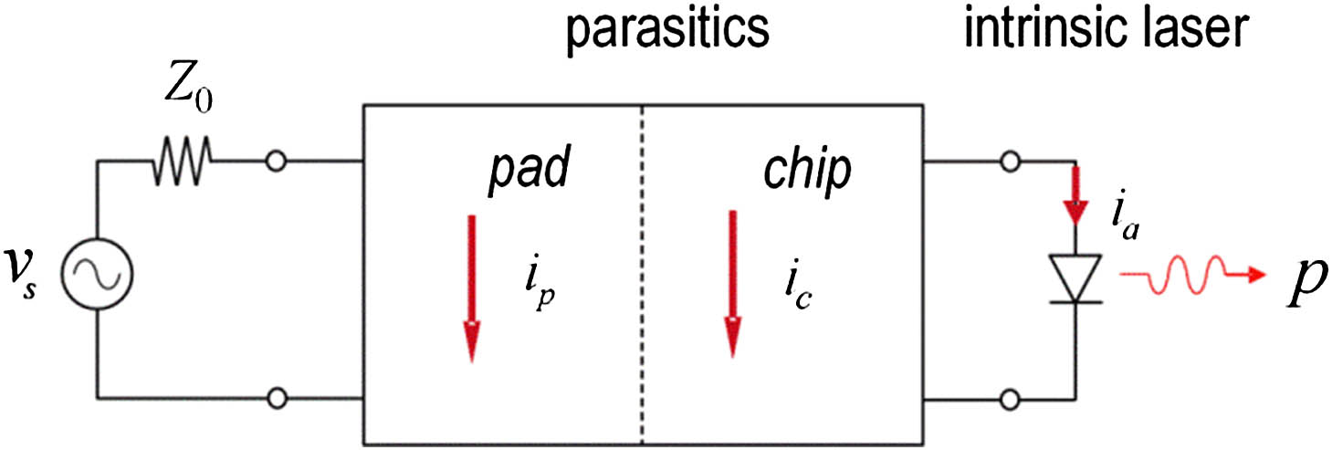
    Fig. 2. Small-signal model of a VCSEL with the high-frequency driving source.
    Schematic of representative optical modes (straight lines) and gain spectra (curves) behavior in a VCSEL as functions of increasing temperature. T0 denotes the typical room temperature.
    Fig. 3. Schematic of representative optical modes (straight lines) and gain spectra (curves) behavior in a VCSEL as functions of increasing temperature. T0 denotes the typical room temperature.
    Simulated PAM4 and on–off keying (OOK) eye diagrams at 40 Gbps with a constant modulation bandwidth of 20 GHz.
    Fig. 4. Simulated PAM4 and on–off keying (OOK) eye diagrams at 40 Gbps with a constant modulation bandwidth of 20 GHz.
    (a) End-to-end coupling between a VCSEL and a PIC based on an SOI platform [115]. A spot-size convertor in the PIC side is always adopted for a high coupling efficiency between the VCSEL and the silicon waveguide. (b) VCSEL coupled to a PIC by 45° micro-reflectors [116]. (c) Grating coupler for coupling between a VCSEL and a PIC [123]. (d) Photonic wire bond for integration for a surface-emitting laser and a PIC [127]. The laser can be a VCSEL or a distributed-feedback surface-emitting laser. PWB, photonic wire bond.
    Fig. 5. (a) End-to-end coupling between a VCSEL and a PIC based on an SOI platform [115]. A spot-size convertor in the PIC side is always adopted for a high coupling efficiency between the VCSEL and the silicon waveguide. (b) VCSEL coupled to a PIC by 45° micro-reflectors [116]. (c) Grating coupler for coupling between a VCSEL and a PIC [123]. (d) Photonic wire bond for integration for a surface-emitting laser and a PIC [127]. The laser can be a VCSEL or a distributed-feedback surface-emitting laser. PWB, photonic wire bond.
    Schematic of a tracking system based on SMI [129,130].
    Fig. 6. Schematic of a tracking system based on SMI [129,130].
    Components of a face recognition module in a modern smartphone. (a) VCSELs for time-of-flight (ToF) proximity sensing and IR illumination. (b) VCSEL array for projection of randomly distributed dots to sense object distance information.
    Fig. 7. Components of a face recognition module in a modern smartphone. (a) VCSELs for time-of-flight (ToF) proximity sensing and IR illumination. (b) VCSEL array for projection of randomly distributed dots to sense object distance information.
    (a) Schematic of focal plane scanning [148,151]. (b) Illustration of structured light [153].
    Fig. 8. (a) Schematic of focal plane scanning [148,151]. (b) Illustration of structured light [153].
    (a) Schematic of an HCG. The red arrows show the direction of wave incidence. The black arrows indicate the E-field direction in both TE and TM polarizations of incidence. (b) Double-mode solution exhibiting perfect intensity cancellation at the HCG output plane leading to 100% reflectivity [159].
    Fig. 9. (a) Schematic of an HCG. The red arrows show the direction of wave incidence. The black arrows indicate the E-field direction in both TE and TM polarizations of incidence. (b) Double-mode solution exhibiting perfect intensity cancellation at the HCG output plane leading to 100% reflectivity [159].
    (a) Schematic of an HCG-VCSEL [160]. (b) HCG-VCSEL array for single-lobe, double-lobe, triple-lobe, “bow-tie,” “sugar cone,” and “doughnut” beam patterns [177]. (c) Schematic of a nanoelectromechanical tunable VCSEL using the highly reflective HCG as its top mirror, instead of conventional DBRs [180]. (d) Schematic of a monolithic HCG-VCSEL array with different HCG parameters.
    Fig. 10. (a) Schematic of an HCG-VCSEL [160]. (b) HCG-VCSEL array for single-lobe, double-lobe, triple-lobe, “bow-tie,” “sugar cone,” and “doughnut” beam patterns [177]. (c) Schematic of a nanoelectromechanical tunable VCSEL using the highly reflective HCG as its top mirror, instead of conventional DBRs [180]. (d) Schematic of a monolithic HCG-VCSEL array with different HCG parameters.
    (a) Schematic of a VCSEL with a silicon HCG as a bottom mirror. An HCG serves as the bottom mirror and potentially serves as a waveguide coupler for an in-plane SOI waveguide, facilitating the integration of a VCSEL with in-plane silicon photonic circuits [188]. (b) Schematic of a vertical-cavity laser with lateral emission into a silicon waveguide via an HCG [189]. (c) Schematic of a vertical-cavity laser with in-plane out-coupling into a SiN waveguide. A subwavelength grating is inserted under a half-VCSEL to redirect the vertical resonance light to the in-plane SiN waveguide [192].
    Fig. 11. (a) Schematic of a VCSEL with a silicon HCG as a bottom mirror. An HCG serves as the bottom mirror and potentially serves as a waveguide coupler for an in-plane SOI waveguide, facilitating the integration of a VCSEL with in-plane silicon photonic circuits [188]. (b) Schematic of a vertical-cavity laser with lateral emission into a silicon waveguide via an HCG [189]. (c) Schematic of a vertical-cavity laser with in-plane out-coupling into a SiN waveguide. A subwavelength grating is inserted under a half-VCSEL to redirect the vertical resonance light to the in-plane SiN waveguide [192].
    Groupλ (nm)Bandwidth (GHz)Bit Rate (Gbps)Temperature (°C)Oxide Aperture (μm)YearRefs.
    IBM85015.4202582001[54]
    Finisar-IBM85019302562008[55]
    CUT85020322592009[56]
    CUT85023402572010[57]
    CUT85028442572012[58]
    CUT85024572582013[59]
    CUT8503050253.52015[60]
    TU Berlin85020302562009[61]
    TU Berlin850402592009[62]
    UIUC85021.2402042014[63]
    UIUC85029.2572552016[64]
    NCU85022.4402542013[65]
    NCU85026412582015[66]
    UCSB980>20352032007[67]
    TU Berlin980442562011[40]
    TU Berlin98024.7502552014[68]
    TU Berlin98026.6522562016[39]
    TU Berlin98035.52532018[69]
    CUT106022502542017[70]
    NEC11002025256.92006[53]
    NEC110024302562007[71]
    NEC110024402562008[72]
    Table 1. Modulation Bandwidths and Bit Rates of VCSELs at Room Temperature Using the Standard On–Off Keying in a Back-to-Back Data Transmission Configuration
    Groupλ (nm)Bandwidth (GHz)Bit Rate (Gbps)Temperature (°C)Oxide Aperture (μm)YearRefs.
    Finisar85010149582012[91]
    Emcore8501628857.52013[92]
    CUT85021408572013[93]
    IBM-CUTa85021509062015[94]
    UIUC85024.5508552016[64]
    NCU85022.4348542013[65]
    NCU85020418582015[66]
    VIS8502515042018[95]
    VIS8502513042018[95]
    TU Berlin980112012032008[97]
    TU Berlin980388562011[40]
    TU Berlin9803012062011[40]
    TU Berlin98023468552014[68]
    TU Berlin98038855.52014[98]
    TU Berlin98018358532014[99]
    TU Berlin98024.5508562016[39]
    CUT106016408542017[70]
    Table 2. Selected Results on Bandwidths and Bit Rates of VCSELs at High Temperatures in an On–Off Keying Modulation Format for Back-to-Back Data Transmission Configuration
    Groupλ (nm)Bit Rate (Gbps)Temperature (°C)Energy eff. (fJ/bit)Oxide Aperture (μm)YearRefs.
    TU Berlin-VIS85025259922011[96]
    TU Berlin-VIS85017256922011[96]
    TU Berlin-VIS8502525563.52012[101]
    TU Berlin850402510842013[104]
    CUT8505025953.52015[60]
    CUT8504025733.52015[60]
    UIUC850402039542014[63]
    NCU85012.52510962011[105]
    NCU850342534562011[105]
    NCU850342510742013[65]
    UCSB980352028632009[67]
    TU Berlin98038851775.52014[98]
    TU Berlin980358513932014[99]
    TU Berlin980352514532015[106]
    Furukawa106010251402011[107]
    Furukawa10602525762014[108]
    CUT1060502510042017[70]
    Table 3. Energy Efficiencies of High-Speed VCSELs with the On–Off Keying Modulation Format in a Back-to-Back Data Transmission Configuration
    Anjin Liu, Philip Wolf, James A. Lott, Dieter Bimberg. Vertical-cavity surface-emitting lasers for data communication and sensing[J]. Photonics Research, 2019, 7(2): 121
    Download Citation