• Photonics Research
  • Vol. 10, Issue 1, 1 (2022)
Shihan Hong1, Long Zhang1, Yi Wang1, Ming Zhang1, Yiwei Xie1, and Daoxin Dai1、2、*
Author Affiliations
  • 1State Key Laboratory for Modern Optical Instrumentation, Center for Optical & Electromagnetic Research, College of Optical Science and Engineering, International Research Center for Advanced Photonics, Zhejiang University, Zijingang Campus, Hangzhou 310058, China
  • 2Ningbo Research Institute, Zhejiang University, Ningbo 315100, China
  • show less
    DOI: 10.1364/PRJ.437726 Cite this Article Set citation alerts
    Shihan Hong, Long Zhang, Yi Wang, Ming Zhang, Yiwei Xie, Daoxin Dai. Ultralow-loss compact silicon photonic waveguide spirals and delay lines[J]. Photonics Research, 2022, 10(1): 1 Copy Citation Text show less
    (a) 3D view of the proposed ultralow-loss and compact silicon photonic waveguide spiral. (b) Enlarged view of tapered Euler-curve S-bend in the middle.
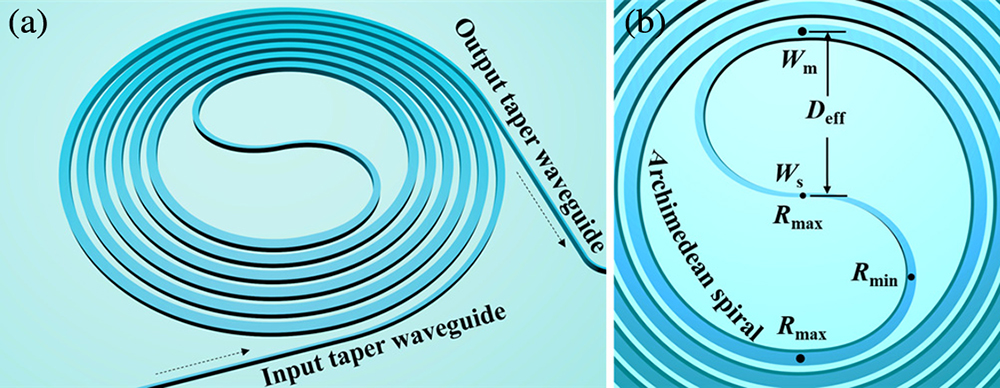
    Fig. 1. (a) 3D view of the proposed ultralow-loss and compact silicon photonic waveguide spiral. (b) Enlarged view of tapered Euler-curve S-bend in the middle.
    Calculated losses due to the (a) top/bottom surface scattering (here σsidewall=0 nm) and (b) sidewall scattering (here σsurface=0 nm). (c) Total scattering loss (here σsurface=0.4 nm).
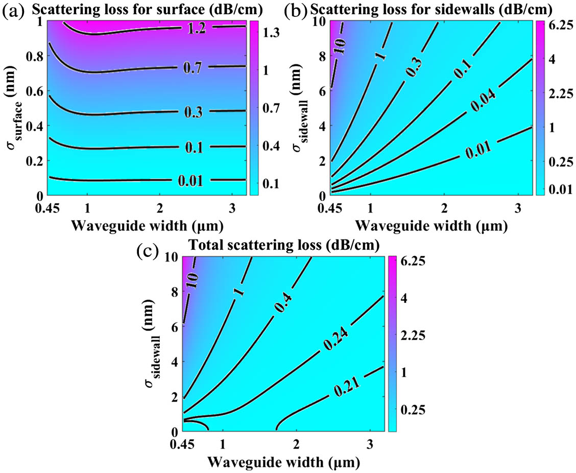
    Fig. 2. Calculated losses due to the (a) top/bottom surface scattering (here σsidewall=0  nm) and (b) sidewall scattering (here σsurface=0  nm). (c) Total scattering loss (here σsurface=0.4  nm).
    Calculated coupling length Lc as the gap width Wgap in the Archimedean spiral varies.
    Fig. 3. Calculated coupling length Lc as the gap width Wgap in the Archimedean spiral varies.
    (a) Calculated excess loss and (b) intermode cross talk as a function of the core width Ws and the bending radius Rmax. Simulated light propagation of the TE0 mode in the (c) tapered Euler-curve S-bend and (d) regular arc S-bend. Calculated excess loss and intermode cross talk at the output port of the (e) tapered Euler S-bend and (f) regular arc S-bend.
    Fig. 4. (a) Calculated excess loss and (b) intermode cross talk as a function of the core width Ws and the bending radius Rmax. Simulated light propagation of the TE0 mode in the (c) tapered Euler-curve S-bend and (d) regular arc S-bend. Calculated excess loss and intermode cross talk at the output port of the (e) tapered Euler S-bend and (f) regular arc S-bend.
    (a) Microscope image of the fabricated 50-cm-long waveguide spiral. (b) Measured transmissions of the waveguide spirals with different lengths L=5, 10, 20, 50, and 100 cm. (c) Measured transmissions of the waveguide spirals on seven chips (rhombus) and linear fit (blue curve). (d) Fitting of theoretical scattering losses (red curve) and measured results (dots).
    Fig. 5. (a) Microscope image of the fabricated 50-cm-long waveguide spiral. (b) Measured transmissions of the waveguide spirals with different lengths L=5, 10, 20, 50, and 100 cm. (c) Measured transmissions of the waveguide spirals on seven chips (rhombus) and linear fit (blue curve). (d) Fitting of theoretical scattering losses (red curve) and measured results (dots).
    (a) Schematic configuration of the n-stage tunable optical delay line. (b) Microscope images of the fabricated tunable delay line chip. (c) Measured optical output waveforms of the tunable delay line system with a time delay of 10–5120 ps. Here the blue curves are the reference signals passing through the corresponding straight waveguide.
    Fig. 6. (a) Schematic configuration of the n-stage tunable optical delay line. (b) Microscope images of the fabricated tunable delay line chip. (c) Measured optical output waveforms of the tunable delay line system with a time delay of 10–5120 ps. Here the blue curves are the reference signals passing through the corresponding straight waveguide.
    ReferenceWaveguide (WG) TypeBitDelay Tuning Range (ps)Resolution (ps)Loss (dB/cm)Footprint (mm2)
    [1]Subwavelength grating silicon WG (Ht=220  nm, Wt=500  nm, Λ=250  nm)1181.94.72.656.55
    [5]Ridge WG (Hr=70  nm, Ht=220  nm, Wt=650  nm)7191.371.422.4713.32
    [4]Thin silicon WG (Ht=60  nm, Wt=1  μm)71280Small (BW = 0.48 nm)0.628.62
    [3]Ridge Si WG (Hr=160  nm, Ht=220  nm, Wt=3  μm)71270100.911.84
    This workBroadened silicon WG (Ht=220  nm, Wt=2  μm)105110100.2812.98
    Table 1. Performance Comparison of On-Chip Tunable Delay Lines Based on Silicon-on-Insulator Waveguidesa
    Shihan Hong, Long Zhang, Yi Wang, Ming Zhang, Yiwei Xie, Daoxin Dai. Ultralow-loss compact silicon photonic waveguide spirals and delay lines[J]. Photonics Research, 2022, 10(1): 1
    Download Citation