• Journal of Infrared and Millimeter Waves
  • Vol. 43, Issue 1, 63 (2024)
Zi-Lu GUO1、2、3, Wen-Juan WANG1、4、**, Hui-Dan QU1, Liu--Yan FAN1, Yi-Cheng ZHU1、2, Ya-Jie WANG5, Chang-Lin ZHENG5, Xing-Jun WANG1, Ping-Ping CHEN1、*, and Wei LU1、2、3、4、***
Author Affiliations
  • 1State Key Laboratory of Infrared Physics,Shanghai Institute of Technology Physics,Chinese Academy of Sciences,Shanghai 200083,China
  • 2University of Chinese Academy of Sciences,Beijing 100049,China
  • 3School of Physical Science and Technology,ShanghaiTech University,Shanghai 201210,China
  • 4Shanghai Research Center for Quantum Sciences,Shanghai 201315,China
  • 5State Key Laboratory of Surface Physics and Department of Physics,Fudan University,Shanghai 200438,China
  • show less
    DOI: 10.11972/j.issn.1001-9014.2024.01.009 Cite this Article
    Zi-Lu GUO, Wen-Juan WANG, Hui-Dan QU, Liu--Yan FAN, Yi-Cheng ZHU, Ya-Jie WANG, Chang-Lin ZHENG, Xing-Jun WANG, Ping-Ping CHEN, Wei LU. Correlation between MBE deoxidation conditions and InGaAs/InP APD performance[J]. Journal of Infrared and Millimeter Waves, 2024, 43(1): 63 Copy Citation Text show less
    Profile diagram and internal electric field distribution of InGaAs/InP APD structure
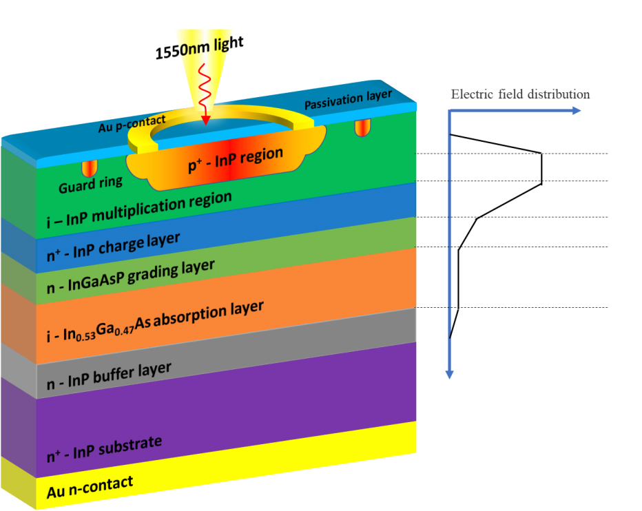
    Fig. 1. Profile diagram and internal electric field distribution of InGaAs/InP APD structure
    Hall carrier concentration and mobility plot
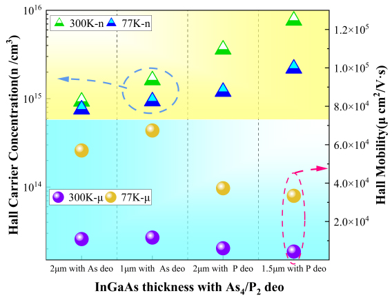
    Fig. 2. Hall carrier concentration and mobility plot
    TRPL spectra of APD wafers
    Fig. 3. TRPL spectra of APD wafers
    (a) Comparison of SIMS depth distributions for Samples via As4, P2 deoxidation,(b) Bulk regions (d = 4.8-5.6 μm) of comparison of deoxidation interface
    Fig. 4. (a) Comparison of SIMS depth distributions for Samples via As4, P2 deoxidation,(b) Bulk regions (d = 4.8-5.6 μm) of comparison of deoxidation interface
    STEM-HAADF image of APD sample A(As-deoxidation)(a)an image of the APD structure on FIB grid,(b)the image of InGaAs and InP buffer,(c)zoom region of InP homojunction interfaces,(d)high-resolution images of the region marked with a red frame in(a)
    Fig. 5. STEM-HAADF image of APD sample A(As-deoxidation)(a)an image of the APD structure on FIB grid,(b)the image of InGaAs and InP buffer,(c)zoom region of InP homojunction interfaces,(d)high-resolution images of the region marked with a red frame in(a)
    STEM-HAADF image of APD sample B(P-deoxidation)(a)an image of the APD structure on the FIB grid,(b)the image of InGaAs and InP buffer,(c)the zoom region of InP homojunction interfaces and stacking fault(circled). Circles indicate dislocations with different core structures,(d)high-resolution images of the area marked with a red frame in(a)
    Fig. 6. STEM-HAADF image of APD sample B(P-deoxidation)(a)an image of the APD structure on the FIB grid,(b)the image of InGaAs and InP buffer,(c)the zoom region of InP homojunction interfaces and stacking fault(circled). Circles indicate dislocations with different core structures,(d)high-resolution images of the area marked with a red frame in(a)
    (a) I-V and gain characteristics of the InGaAs/InP APD,(b) TRPL spectra of ARC-APD
    Fig. 7. (a) I-V and gain characteristics of the InGaAs/InP APD,(b) TRPL spectra of ARC-APD
    SampleOCHSiN
    A2.25E+179.76E+182.08E+181.56E+171.86E+16
    B8E+179.09E+181.34E+183.74E+176.61E+16
    DL1E151E151E161E145E14
    Table 1. Average peak concentrations (cm-3 ) of impurities in bulk regions (d = 4.8-5.6 μm) from SIMS measurements.
    Zi-Lu GUO, Wen-Juan WANG, Hui-Dan QU, Liu--Yan FAN, Yi-Cheng ZHU, Ya-Jie WANG, Chang-Lin ZHENG, Xing-Jun WANG, Ping-Ping CHEN, Wei LU. Correlation between MBE deoxidation conditions and InGaAs/InP APD performance[J]. Journal of Infrared and Millimeter Waves, 2024, 43(1): 63
    Download Citation