• Photonics Research
  • Vol. 8, Issue 4, 548 (2020)
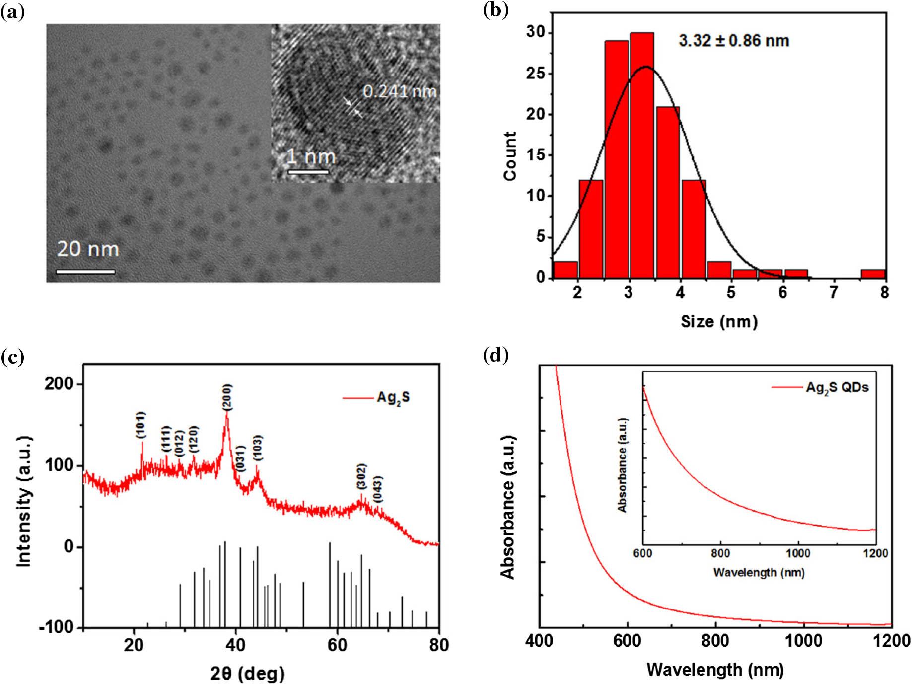
Bin Wang1、2, Chen Zhao1、2, Huanyu Lu2、3, Tingting Zou1、2, Subhash C. Singh1、4、5、*, Zhi Yu1、6、*, Chaonan Yao1、2, Xin Zheng1、2, Jun Xing1、2, Yuting Zou1、2, Cunzhu Tong3, Weili Yu1, Bo Zhao1, and Chunlei Guo1、4、7、*
Author Affiliations
  • 1The Guo China-US Photonics Laboratory, State Key Laboratory of Applied Optics, Changchun Institute of Optics, Fine Mechanics and Physics, Chinese Academy of Sciences, Changchun 130033, China
  • 2University of Chinese Academy of Sciences, Beijing 100049, China
  • 3State Key Laboratory of Luminescence and Applications, Changchun Institute of Optics, Fine Mechanics and Physics, Chinese Academy of Sciences, Changchun 130033, China
  • 4The Institute of Optics, University of Rochester, Rochester, New York 14627, USA
  • 5e-mail: ssingh49@ur.rochester.edu
  • 6e-mail: zhiyu@ciomp.ac.cn
  • 7e-mail: guo@optics.rochester.edu
  • show less
    DOI: 10.1364/PRJ.383612 Cite this Article Set citation alerts
    Bin Wang, Chen Zhao, Huanyu Lu, Tingting Zou, Subhash C. Singh, Zhi Yu, Chaonan Yao, Xin Zheng, Jun Xing, Yuting Zou, Cunzhu Tong, Weili Yu, Bo Zhao, Chunlei Guo. SERS study on the synergistic effects of electric field enhancement and charge transfer in an Ag2S quantum dots/plasmonic bowtie nanoantenna composite system[J]. Photonics Research, 2020, 8(4): 548 Copy Citation Text show less
    Characterization of Ag2S QDs. (a) TEM image of Ag2S QDs (scale bar 20 nm). Inset shows an HRTEM image of a QD with a lattice spacing of 0.241 nm (scale bar 1 nm). (b) Histogram for the size distribution of Ag2S QDs with average size of 3.32 nm. (c) XRD spectrum of the Ag2S QDs with JCPDS data. (d) UV-vis-NIR absorption spectra of the Ag2S QDs.
    Fig. 1. Characterization of Ag2S QDs. (a) TEM image of Ag2S QDs (scale bar 20 nm). Inset shows an HRTEM image of a QD with a lattice spacing of 0.241 nm (scale bar 1 nm). (b) Histogram for the size distribution of Ag2S QDs with average size of 3.32 nm. (c) XRD spectrum of the Ag2S QDs with JCPDS data. (d) UV-vis-NIR absorption spectra of the Ag2S QDs.
    Characterization of Au BNA arrays. (a) SEM images of the BNA arrays (scale bar 2 μm). Inset shows an enlarged view of three pairs of BNA (scale bar 300 nm). (b) EDS analysis of Ag2S QDs on BNA arrays. On the top, from left to right: (i) scanned region for EDS, and elemental mapping of (ii) S, (iii) Ag, and (iv) Au. Inset shows the elemental composition of different elements in BNA arrays/Ag2S-QDs substrate.
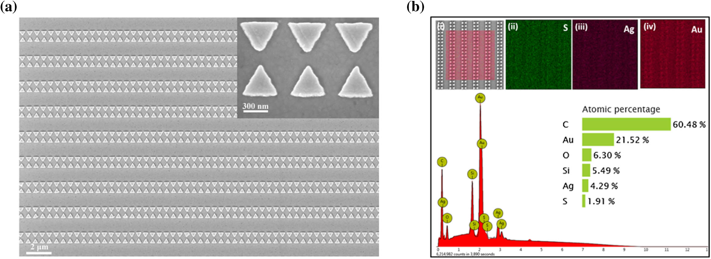
    Fig. 2. Characterization of Au BNA arrays. (a) SEM images of the BNA arrays (scale bar 2 μm). Inset shows an enlarged view of three pairs of BNA (scale bar 300 nm). (b) EDS analysis of Ag2S QDs on BNA arrays. On the top, from left to right: (i) scanned region for EDS, and elemental mapping of (ii) S, (iii) Ag, and (iv) Au. Inset shows the elemental composition of different elements in BNA arrays/Ag2S-QDs substrate.
    Schematics and calculated E-field distribution of Au BNA arrays. (a) Geometrical parameters of BNA arrays with MIM structure. (b) E-field enhancement of the BNA arrays at P0 point. Inset shows the enlarged E-field enhancement spectrum range from 780 to 930 nm. (c)–(e) E-field distribution (|E|2/|E0|2) in x–y plane at three LSPR modes.
    Fig. 3. Schematics and calculated E-field distribution of Au BNA arrays. (a) Geometrical parameters of BNA arrays with MIM structure. (b) E-field enhancement of the BNA arrays at P0 point. Inset shows the enlarged E-field enhancement spectrum range from 780 to 930 nm. (c)–(e) E-field distribution (|E|2/|E0|2) in xy plane at three LSPR modes.
    Raman spectra of PATP molecules adsorbed on a different substrate. (a)–(c) Raman spectra of PATP molecules adsorbed on Ag2S QDs coated BNA arrays (red curve), BNA arrays (black curve), and Ag2S QDs (blue curve), respectively. (d) Raman spectrum of PATP powder as reference. The spectra were collected under 785 nm laser excitation. Raman spectra are shifted compared to each other along the y axis for better viewing.
    Fig. 4. Raman spectra of PATP molecules adsorbed on a different substrate. (a)–(c) Raman spectra of PATP molecules adsorbed on Ag2S QDs coated BNA arrays (red curve), BNA arrays (black curve), and Ag2S QDs (blue curve), respectively. (d) Raman spectrum of PATP powder as reference. The spectra were collected under 785 nm laser excitation. Raman spectra are shifted compared to each other along the y axis for better viewing.
    Raman spectra of PATP molecules adsorbed on Au film and BNA substrates and the spatial E-field distribution of the BNA. (a) Raman spectra of the PATP molecules adsorbed on the BNA arrays (red curve) and 30 nm Au film (blue curve) under 785 nm laser excitation. (b), (c) Spatial E-field distribution (|E|2/|E0|2) of the BNA in the x–y and x–z planes under 785 nm laser excitation, respectively. (d), (e) Spatial distribution of E-field EF corresponding to 1078 cm−1 (or 857 nm) and 1140 cm−1 (or 862 nm) vibrational modes of PATP in the x–y plane and x–z plane, respectively. In the plots (d) and (e), the white dashed lines represent the BNA for the SERS E-field EF calculation; the excitation wavelength was considered as 785 nm. Raman spectra are shifted compared to each other along the y axis for better viewing.
    Fig. 5. Raman spectra of PATP molecules adsorbed on Au film and BNA substrates and the spatial E-field distribution of the BNA. (a) Raman spectra of the PATP molecules adsorbed on the BNA arrays (red curve) and 30 nm Au film (blue curve) under 785 nm laser excitation. (b), (c) Spatial E-field distribution (|E|2/|E0|2) of the BNA in the xy and xz planes under 785 nm laser excitation, respectively. (d), (e) Spatial distribution of E-field EF corresponding to 1078  cm1 (or 857 nm) and 1140  cm1 (or 862 nm) vibrational modes of PATP in the xy plane and xz plane, respectively. In the plots (d) and (e), the white dashed lines represent the BNA for the SERS E-field EF calculation; the excitation wavelength was considered as 785 nm. Raman spectra are shifted compared to each other along the y axis for better viewing.
    Energy level diagram of (a) Ag2S-QDs/PATP, (b) Au-BNA/PATP, and (c) BNA/Ag2S-QDs/PATP systems under 785 nm laser excitation, respectively.
    Fig. 6. Energy level diagram of (a) Ag2S-QDs/PATP, (b) Au-BNA/PATP, and (c) BNA/Ag2S-QDs/PATP systems under 785 nm laser excitation, respectively.
    Raman spectra and degree of charge transfer of different composite systems. (a) Raman spectra of the PATP molecule adsorbed on Ag2S QDs coated BNA arrays (red curve) and Ag2S QDs coated Au thin film (30 nm) (blue curve). (b) Degree of charge transfer (ρCT) of the PATP adsorbed on Ag2S coated Au film and Ag2S coated BNA arrays at b2 modes with excitation at 785 nm. Raman spectra are shifted compared to each other along the y axis for better viewing. Error bars represent [mean±SD, (n=5)].
    Fig. 7. Raman spectra and degree of charge transfer of different composite systems. (a) Raman spectra of the PATP molecule adsorbed on Ag2S QDs coated BNA arrays (red curve) and Ag2S QDs coated Au thin film (30 nm) (blue curve). (b) Degree of charge transfer (ρCT) of the PATP adsorbed on Ag2S coated Au film and Ag2S coated BNA arrays at b2 modes with excitation at 785 nm. Raman spectra are shifted compared to each other along the y axis for better viewing. Error bars represent [mean±SD, (n=5)].
    SERS spectra and E-field distribution with polarization angles. SERS spectra of PATP adsorbed onto (a) BNA arrays and (b) Ag2S coated BNA arrays with different polarization angles under 785 excitation, respectively. Insets show the directions of θpola=0° and θpola=90°, and the polarization angle changes in the counterclockwise direction. (c) SERS intensity at 1078 cm−1 [ν(CS), a1] in BNA/PATP system, 1075 cm−1 [ν(CS), a1] and 1138 cm−1 [δ(CH), b2] in BNA/QDs/PATP system with different polarization angles. (d) Degree of charge transfer (ρCT) at 1138 cm−1 in BNA/Ag2S/PATP system with different polarization angles. Spatial E-field distribution of BNA arrays in the (e) x–y plane and(f) x–z plane with different polarization angles under 785 excitation, respectively. Raman spectra are shifted compared to each other along the y axis for better viewing. Error bars represent [mean±SD, (n=5)].
    Fig. 8. SERS spectra and E-field distribution with polarization angles. SERS spectra of PATP adsorbed onto (a) BNA arrays and (b) Ag2S coated BNA arrays with different polarization angles under 785 excitation, respectively. Insets show the directions of θpola=0° and θpola=90°, and the polarization angle changes in the counterclockwise direction. (c) SERS intensity at 1078  cm1 [ν(CS), a1] in BNA/PATP system, 1075  cm1 [ν(CS), a1] and 1138  cm1 [δ(CH), b2] in BNA/QDs/PATP system with different polarization angles. (d) Degree of charge transfer (ρCT) at 1138  cm1 in BNA/Ag2S/PATP system with different polarization angles. Spatial E-field distribution of BNA arrays in the (e) xy plane and(f) xz plane with different polarization angles under 785 excitation, respectively. Raman spectra are shifted compared to each other along the y axis for better viewing. Error bars represent [mean±SD, (n=5)].
    XPS characterization of Ag2S QDs. (a), (b) Overall and Ag 3d of Ag2S coated BNA arrays, respectively. (c), (d) S 2p of Ag2S coated BNA arrays with and without PATP molecule, respectively.
    Fig. 9. XPS characterization of Ag2S QDs. (a), (b) Overall and Ag 3d of Ag2S coated BNA arrays, respectively. (c), (d) S 2p of Ag2S coated BNA arrays with and without PATP molecule, respectively.
    Calculated distribution of E-field under three modes. (a)–(c) Spatial E-field distribution at a wavelength of 802 nm (LSPR1), 726 nm (LSPR2), and 686 nm (LSPR3) in the x–z plane, respectively. (d)–(f) The line distribution of E-field enhancement at 802 nm (LSPR1 mode) along x, y, and z direction, respectively. Inset figures show the assumed direction of x, y, and range of height (h).
    Fig. 10. Calculated distribution of E-field under three modes. (a)–(c) Spatial E-field distribution at a wavelength of 802 nm (LSPR1), 726 nm (LSPR2), and 686 nm (LSPR3) in the xz plane, respectively. (d)–(f) The line distribution of E-field enhancement at 802 nm (LSPR1 mode) along x, y, and z direction, respectively. Inset figures show the assumed direction of x, y, and range of height (h).
    Calculation of enhancement factor in the BNA/Ag2S-QDs/PATP system under 785 nm laser excitation. (a) Depth-dependent Raman intensity of the single Si wafer at the 520.7 cm−1 band under 785 nm laser excitation. A pinhole size of 100 μm and a 100× working-length objective is used. (b) Raman spectra of PATP powder and PATP with BNA/Ag2S-QDs composite substrate. (c) Raman spectra of PATP powder, and PATP with BNA and Au/Ag2S-QDs composite substrate. (d) Raman intensity of bands at 1075 cm−1 (a1) and 1138 cm−1 (b2) in BNA/Ag2S-QDs/PATP, BNA/PATP, and Au/Ag2S-QDs/PATP systems. Raman spectra are shifted compared to each other along the y axis for better viewing. Error bars represent [mean±SD, (n=5)].
    Fig. 11. Calculation of enhancement factor in the BNA/Ag2S-QDs/PATP system under 785 nm laser excitation. (a) Depth-dependent Raman intensity of the single Si wafer at the 520.7  cm1 band under 785 nm laser excitation. A pinhole size of 100 μm and a 100× working-length objective is used. (b) Raman spectra of PATP powder and PATP with BNA/Ag2S-QDs composite substrate. (c) Raman spectra of PATP powder, and PATP with BNA and Au/Ag2S-QDs composite substrate. (d) Raman intensity of bands at 1075  cm1 (a1) and 1138  cm1 (b2) in BNA/Ag2S-QDs/PATP, BNA/PATP, and Au/Ag2S-QDs/PATP systems. Raman spectra are shifted compared to each other along the y axis for better viewing. Error bars represent [mean±SD, (n=5)].
    Mapping of SERS spectrum and E-field distribution. (a) Camera view of scanning area (left side) and mapping of SERS spectrum at 1138 cm−1 corresponding to the scanning area (right side). (b) Spatial E-field distribution (|E|2/|E0|2) of BNA arrays under 785 nm excitation.
    Fig. 12. Mapping of SERS spectrum and E-field distribution. (a) Camera view of scanning area (left side) and mapping of SERS spectrum at 1138  cm1 corresponding to the scanning area (right side). (b) Spatial E-field distribution (|E|2/|E0|2) of BNA arrays under 785 nm excitation.
    Raman spectra of PATP molecule adsorbed on different substrates. (a) Comparison of Raman spectra of PATP molecule adsorbed on the Ag2S QDs under 473 and 532 nm laser excitation. (b), (c) Raman spectra of PATP molecule adsorbed on BNA, Ag2S QDs, and Ag2S QDs coated BNA under 473 and 532 nm laser excitation, respectively. (d) Comparison of Raman spectra of PATP molecule adsorbed on Ag2S QDs coated BNA arrays under 473 and 532 nm laser excitation. (e), (f) Degree of charge transfer (ρCT) of PATP absorbed on Ag2S QDs and Ag2S QDs coated BNA arrays substrate at b2 modes with excitation at 473 and 532 nm, respectively. Raman spectra are shifted compared to each other along the y axis for better viewing. Error bars represent [mean±SD, (n=5)].
    Fig. 13. Raman spectra of PATP molecule adsorbed on different substrates. (a) Comparison of Raman spectra of PATP molecule adsorbed on the Ag2S QDs under 473 and 532 nm laser excitation. (b), (c) Raman spectra of PATP molecule adsorbed on BNA, Ag2S QDs, and Ag2S QDs coated BNA under 473 and 532 nm laser excitation, respectively. (d) Comparison of Raman spectra of PATP molecule adsorbed on Ag2S QDs coated BNA arrays under 473 and 532 nm laser excitation. (e), (f) Degree of charge transfer (ρCT) of PATP absorbed on Ag2S QDs and Ag2S QDs coated BNA arrays substrate at b2 modes with excitation at 473 and 532 nm, respectively. Raman spectra are shifted compared to each other along the y axis for better viewing. Error bars represent [mean±SD, (n=5)].
    Band AssignmentPATP/Ag2S-QDs/BNA/cm1PATP/BNA/cm1PATP/cm1
    γ(CC)+γ(CCC), 18a (a1)100410041007
    ν(CS), 7a (a1)107510781084
    δ(CH), 9b (b2)11381140
    δ(CH), 9a (a1)118411801175
    1229
    ν(CC)+δ(CH), 14 (b2)1299
    δ(CH)+ν(CC), 3 (b2)13881389
    ν(CC)+δ(CH), 19 (b2)14351433
    ν(CC), 8b (b2)1574
    ν(CC), 8a (a1)15831590
    Table 1. Raman Peak Assignment in the SERS Spectrum of the PATP-Modified SERS Substrate
    Bin Wang, Chen Zhao, Huanyu Lu, Tingting Zou, Subhash C. Singh, Zhi Yu, Chaonan Yao, Xin Zheng, Jun Xing, Yuting Zou, Cunzhu Tong, Weili Yu, Bo Zhao, Chunlei Guo. SERS study on the synergistic effects of electric field enhancement and charge transfer in an Ag2S quantum dots/plasmonic bowtie nanoantenna composite system[J]. Photonics Research, 2020, 8(4): 548
    Download Citation