Xiang Li, Degang Zhao. Effectiveness of inserting an InGaN interlayer to improve the performances of InGaN-based blue-violet laser diodes[J]. Chinese Optics Letters, 2016, 14(6): 062502
Copy Citation Text
Electron leakage still needs to be solved for InGaN-based blue-violet laser diodes (LDs), despite the presence of the electron blocking layer (EBL). To reduce further electron leakage, a new structure of InGaN-based LDs with an InGaN interlayer between the EBL and -type waveguide layer is designed. The optical and electrical characteristics of these LDs are simulated, and it is found that the adjusted energy band profile in the new structure can improve carrier injection and enhance the effective energy barrier against electron leakage when the In composition of the InGaN interlayer is properly chosen. As a result, the device performances of the LDs are improved.
InGaN-based laser diodes (LDs) and light-emitting diodes have attracted much attention since the 1990s because of their potential uses as violet, blue, and green coherent light sources[1–6]. However, InGaN-based blue-violet LDs have suffered from severe electron leakage owing to the polarization effect and weak confinement capability of electrons within their shallow quantum wells (QWs). As a result of the polarization charges, the conduction band on the -side is higher than the conduction band on the -side. The electrons are prone to skipping across QWs, causing electron leakage. The percentage of electron leakage current is defined as the ratio of the electron current that overflowed into the -type layer to the total electron current injected into the QWs of the LDs. In addition, since fewer holes are injected into QWs induced by the poor holes’ injection efficiency, excess electrons cannot recombine in the QWs very well. The excess electrons are transported into the -type region and then recombine with the holes there. As a result, the problem of the electron leakage will be further exacerbated, especially at high injection currents, which will result in carrier loss and reduced quantum efficiency.
To alleviate electron leakage, a conventional design was used where a 20 nm electron blocking layer (EBL) was inserted between the last quantum barrier (LQB) of the active region and the -type waveguide layer. However, this approach is subject to the positive polarization charge localized at the interface between the LQB and the EBL[7]. The positive interface charge can drop the conduction band edge near the LQB/EBL interface and lower the effective electron barrier. As a result, they are unfavorable for blocking electron leakage. Moreover, an EBL might act as a potential barrier for holes and increase the difficulty of hole injection[8,9]. To solve these problems and increase the effectiveness of EBL, several suggestions about the design of EBL have been reported, including an AlGaN/GaN multi-quantum-barriers EBL[10,11], a polarization-matched AlInGaN EBL[12], and a grading or tapered AlGaN EBL[13–16].
In this work, an InGaN interlayer between the EBL and the -type waveguide layer in a new structure is proposed to adjust the energy band profile and improve the device performance of InGaN-based blue-violet LDs. The electrical and optical characteristics of both the new and reference LD structures (i.e., with and without the InGaN interlayer) are calculated and analyzed with numerical simulations.
Sign up for Chinese Optics Letters TOC. Get the latest issue of Chinese Optics Letters delivered right to you!Sign up now
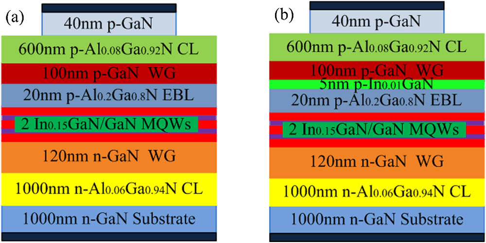
To analyze the effects of the new structure, there are two different LD structures in our study, as shown in Fig. 1. It is shown in Fig. 1(a) that the reference structure without any additional InGaN interlayer (denoted as Ref. LD) is composed of a 1 μm GaN substrate (Si: ), a 1 μm -type cladding layer (Si: ), a 120 nm -type GaN lower waveguide layer (Si: ), the multi-quantum-wells (MQWs) active region, a 20 nm -type EBL (Mg: ), a 100 nm -type GaN upper waveguide layer (Mg: ), a 0.6 μm -type cladding layer (Mg: ), and a 40 nm -type GaN (Mg: ) contact layer. The MQWs consist of two 2.5 nm un-doped well layers and three 14 nm un-doped barrier layers. Figure 1(b) shows the structure of the new LD with an inserted InGaN interlayer (denoted as New LD), which is quite similar to that of Ref. LD except for the -type region. An additional 5 nm un-doped is inserted between the EBL and the -type upper waveguide layer. The cavity length of the LDs is 600 μm and the width of the ridge is 2 μm. The depth of the ridge is 40 nm. The reflectivity of both end mirrors is taken as 0.19. The lateral width of the LDs is 10 μm.
Figure 1.Schematic diagrams of (a) the Ref. LD and (b) the New LD structures with ridge waveguides.
Here, LASTIP software from Crosslight Software Inc. is employed to acquire the electrical and optical characteristics of the LDs. The simulator is based on the finite element analysis of the drift-diffusion model with full Fermi–Dirac statistics for the current continuity equations as well as for the Poisson equation, including the effect of polarization charges in two-dimensions[17]. The built-in polarization induced by spontaneous and piezoelectric polarizations is considered at heterointerfaces of nitride-related devices[18]. In order to consider the built-in polarization within the interfaces of nitride devices in the actual simulation, the electric field caused by the spontaneous and piezoelectric polarization has to be added to the original electric field, including the ionized dopants and the free carrier-induced electric field. As a result, the total electric field in the device is modulated by polarization charges. The built-in polarization charge density at each heterointerface is calculated using the parameters given by Fiorentini et al. Specifically, the spontaneous polarization of ternary nitride alloys can be expressed by As for the piezoelectric polarizations of AlInGaN, InGaN, and AlGaN, they can be estimated by the following expressions where and are the lattice constants of the substrate and the epitaxial layer. The total built-in polarization is the sum of the spontaneous and piezoelectric polarizations. The polarization factor due to the partial compensation of the built-in polarization by charged defects was set to be 50%. In the numerical calculation, the activation energy of the Mg acceptor is taken as 170 meV for GaN, which is assumed to increase 3 meV per 1% of the Al increment for AlGaN alloy[19]. The absorption coefficient of Mg-doped GaN depends on dthe oping concentration of Mg, as reported in Ref. [20], and the absorption coefficients of weakly Si-doped and un-doped GaN are taken as . The absorption coefficient of heavily doped -type GaN is taken as . For AlGaN and InGaN, the absorption coefficients are taken approximately to be the same as GaN.
The calculated P-I-V diagrams of Ref. LD and New LD are shown in Fig. 2. As for the I-V curves, the threshold voltages of the two LDs are nearly identical, with a value of 3 V, while the series resistances of the Ref. LDs and New LDs are quite different. For the Ref. LD, the series resistance is 21 Ω, while it is 15 Ω for the New LD, 29% lower than that of the Ref. LD, which is attributed to the lower energy band of the -type region in the New LD. The lower energy band of the -type region needs less applied voltage, which results in a smaller series resistance. As for P-I curves, the threshold current of the new structure is smaller than that of the reference structure, which is consistent with the theoretical analysis and prediction mentioned above. For the Ref. LD, the threshold current is 36 mA, while it is 32 mA for the New LD, 11% lower than the Ref. LD. On the other hand, the slope efficiency of the Ref. LD is 0.9 W/A, while it is 1.1 W/A for New LD, 22% higher than that of the Ref. LD. At the same current of 120 mA, the operation voltage and output light power of the Ref. LD is 5.2 V and 77 mW, while they are 4.9 V and 99 mW for the New LD, respectively. The wall-plug efficiencies of the Ref. LDs and New LD are derived to be 12.3% and 16.8%, respectively. It is evident that the optical and electrical performances of the LD with the new structure are remarkably enhanced.
Figure 2.Output power and voltage versus current of the Ref. LD (black) and the New LD (red).
Because the InGaN interlayer is very thin, the optical field in the InGaN interlayer is rather small, which has little effect on the optical field distribution of the New LD compared to the Ref. LD. Therefore, we only consider the influence of the thin InGaN interlayer on the electric characteristics in this work. To analyze the reasons for the improved performances, the energy band diagrams of the Ref. LD and the New LD structure at an injection current of 120 mA are shown in Fig. 3. As shown in Fig. 3(a) and 3(b), and are the effective EBL energy barriers for electrons and holes, respectively. The effective electron energy barrier for the holes is reduced from 195 meV for the Ref. LD to 176 meV for the New LD. The reason for the reduction is as follows: in the New LD with an additional thin interlayer between the EBL and the -type waveguide layer, the built-in valence band offset () of the EBL is increased and forms an unintentional well on the right-hand side (RHS) of the EBL. As a result, the hole’s quasi-Fermi level is easily pulled into the valence band due to the hole accumulation captured by the well. Moreover, the valence band bending of the interlayer is downward due to the existence of a negative polarization charge at the interface between the EBL and the interlayer, which promotes further the entry of the hole’s quasi-Fermi level into the valence band. As a result, the energy barrier for the hole injection is decreased, and then the difficulty of hole injection is reduced. It is found that the effective EBL energy barrier for electrons is now , which is much higher than the barrier height in Ref. LD (). The rise in the effective EBL energy barrier for electrons is closely related to the reduction of the total electrical field at the EBL. It is noted that the band edge profile strongly deviates from the ideal rectangular shape, which is due to the presence of interface polarization charges, ionized impurities, free carriers, and applied bias. Therefore, the total electric field at the EBL could be expressed by where , , , and are the electric fields by the external applied bias, the built-in electric field due to the ionized dopants, the free carrier-induced electric field, and the electric field caused by the spontaneous and piezoelectric polarizations, respectively. Note that the component of is not illustrated in Fig. 3(a). Though is somehow related to and should not be treated individually in such a self-consistent Schodinger–Poisson solver, it would not change the dependence tendency of on [21,22]. In the Ref. LD structure, a net negative polarization charge is located on the RHS of the EBL due to the intense spontaneous and piezoelectric polarization. In the New LD with a thin interlayer between the EBL and the -type waveguide layer, the negative polarization charge introduced by the interlayer is added at the RHS of the EBL. More negative polarization charges will accumulate on the RHS of the EBL, and thus the polarization-induced electric field at the EBL close to the interlayer is enhanced as compared with that of the Ref. LD. Therefore, the total electric field at the EBL is weakened according to Eq. (4), and the energy band inclination is reduced. As a result, the energy band of the whole -type region is lowered relative to the -type region, and thus the effective barrier height of the EBL for electrons is increased. Consequently, the energy band profile of the New LD is improved by inserting the thin interlayer, which results in reduced electron leakage and will improve the device performance.
Figure 3.Energy band diagrams of (a) the Ref. LD and (b) the New LD structures (black lines) at 120 mA. Symbols + and − represent positive and negative polarization charges. The red lines mark the quasi-Fermi levels and . The effective potential heights for electrons and holes are marked.
In Fig. 4, the vertical electron current density versus the distance surrounding the active region is plotted for both structures at 120 mA. It is clearly noted that the electrons are injected from the -side into the QWs and then recombined with the holes, which results in the decrease of electron current density along the distance of transportation. It is found that for the Ref. LD, the injected electron current density is smaller than that of the New LD, since the energy band of the -type region for the New LD is lower and more electrons can be easily transported and injected into QWs. For the Ref. LD, the reduction of the electron current density in the QWs is smaller than that of the New LD. In the New LD, the electron leakage is remarkably reduced owing to the increase of the effective EBL energy barrier for electrons. The improved hole injection will also be in favor of enhancing the electrons’ recombination probability of holes in QWs, which will further reduce the electron leakage. Specifically, 25% of the injected electrons leak into the -type region in the Ref. LD, while such an electron leakage current is reduced to 6% in the New LD. This result provides clear evidence that it is efficient to suppress electron leakage by employing the New LD structure. In addition, it is noted that an escalation of electron leakage from QWs to the -type region will be presented in the Ref. LD when the injection current is increased.
Figure 4.Vertical electron current density distribution along growth direction surrounding the active region for Ref. (black) and New (red) LDs at 120 mA.
Figure 5 demonstrates electron and hole concentration distribution around the active region for the Ref. LD and New LD at 120 mA. It is found that the electron and hole concentrations in the QWs of the New LD are relatively lower than those of the Ref. LD. In both LDs, the electron and hole concentrations of the upper QW close to the -side are higher than those in the lower QW, which makes most of injected carriers recombine in the upper QW close to the -side. A notable accumulation of holes on the RHS of the EBL for both LDs is seen in Fig. 5(b), and it becomes more severe after the thin InGaN layer is inserted into the New LD. In fact, in the New LD with an additional thin InGaN interlayer, the built-in valence band offset () can form an unintentional shallow triangle well on the RHS of the EBL to capture more holes. The hole accumulation brought by the InGaN interlayer will have a negative influence on the device performance. Therefore, the negative effect should be minimized as much as possible by optimizing the InGaN interlayer for the New LD.
Figure 5.(a) Electron and (b) hole concentration distribution around the active region for Ref. LD (black) and New LD (red) at 120 mA.
The effects of indium composition in the interlayer on hole accumulation and electron leakage are investigated. Figure 6 shows the percentage of electron leakage current and the RHS hole density of the EBL with indium composition of the interlayer varying from 0% to 4% at 120 mA, except where the point at zero composition of indium is marked as the Ref. LD without an InGaN interlayer for comparison. Compared to the Ref. LD with an InGaN interlayer, the electron leakage of the New LD is smaller when is increased to 4%, proving the validity of the new structure. The reduced electron leakage is attributed to the improved barrier for electron and hole injection. Specifically, when is reduced to 1%, the electron leakage current reaches a minimal value because the EBL energy barrier for electrons plays a role and the hole injection is improved. However, the electron leakage is increased from 6% to 18% when increases from 1% to 4%. The deteriorated electron leakage is attributed to the rapidly increased hole accumulation, which becomes the dominated limiting factor. In fact, as the indium composition increases, the valence band offset of the interlayer is enlarged and the unintentional triangle well on the RHS of the EBL becomes deeper. As a result, more holes are captured and wasted in the well, and the hole injection efficiency is reduced. More excess electrons cannot recombine with holes in the active region and are transported into the -type region to recombine with holes there and then form a severe electron leakage. Figure 7 illustrates the slope efficiency and threshold current of the device versus the indium composition of the interlayer; the middle inset describes the relationship between the output power and indium composition at 120 mA. When the indium composition of the interlayer is about 1%, the device performances, including slope efficiency, threshold current, and output power, achieve optimal values, which is a comprehensive improvement resulting in a modulated, improved energy band profile and the suppression of unwanted hole accumulation.
Figure 6.Percentage of electron leakage current (black) and RHS hole density of the EBL (red) with varying indium composition of at 120 mA except where the point at zero composition of indium is marked as Ref. LD without an InGaN interlayer for comparison.
Figure 7.Slope efficiency (black) and threshold current (red) of the device versus indium composition of interlayer; the middle inset describes the relationship between the output power and indium composition at 120 mA.
In conclusion, we design a new LD structure by inserting an InGaN layer with an optimized In composition between the EBL and the -type waveguide layer. The optical and electrical characteristics of the LDs with the new and reference structures are theoretically calculated and analyzed. It is found that the energy band profile is modulated. The improved carrier injection and the adjusted effective energy barrier can be effective against electron leakage. Finally, it is found that by additionally introducing the InGaN layer, the energy band of the whole -type region is lowered relative to the -type region, and thus the effective barrier height for electrons between the LQB layer and the EBL is increased. It is also found that the hole injection is improved, especially when the choice of the In composition in the InGaN interlayer is optimized. As a result, the electron leakage current is reduced dramatically, and thus the performances of the new LDs, including threshold current density, slope efficiency, and output power, are improved.
References
[1] L. C. Le, D. G. Zhao, D. S. Jiang, P. Chen, Z. S. Liu, J. Yang, X. G. He, X. J. Li, J. P. Liu, J. P. Liu, J. J. Zhu, S. M. Zhang, H. Yang. Opt. Express, 22, 10(2014).
[10] S.-N. Lee, S. Y. Cho, H. Y. Ryu, J. K. Son, H. S. Paek, T. Sakong, T. Jang, K. K. Choi, K. H. Ha, M. H. Yang, O. H. Nam, Y. Park, E. Yoon. Appl. Phys. Lett., 88, 111101(2006).
Xiang Li, Degang Zhao. Effectiveness of inserting an InGaN interlayer to improve the performances of InGaN-based blue-violet laser diodes[J]. Chinese Optics Letters, 2016, 14(6): 062502