
Zhengwu Shu, Lei Jiang, Xingxing Hu, Yue Xu. An integrated front-end vertical hall magnetic sensor fabricated in 0.18 μm low-voltage CMOS technology[J]. Journal of Semiconductors, 2022, 43(3): 032402
- Journal of Semiconductors
- Vol. 43, Issue 3, 032402 (2022)
Abstract
1. Introduction
Due to their full compatibility with CMOS technologies, Hall sensors have been widely applied in many different fields such as industrial control systems, computers, automobiles, and consumer electronics, where magnetic field detection or contactless measurement are required[
In the past few decades, many attempts of fabricating vertical Hall sensors have been undertaken[
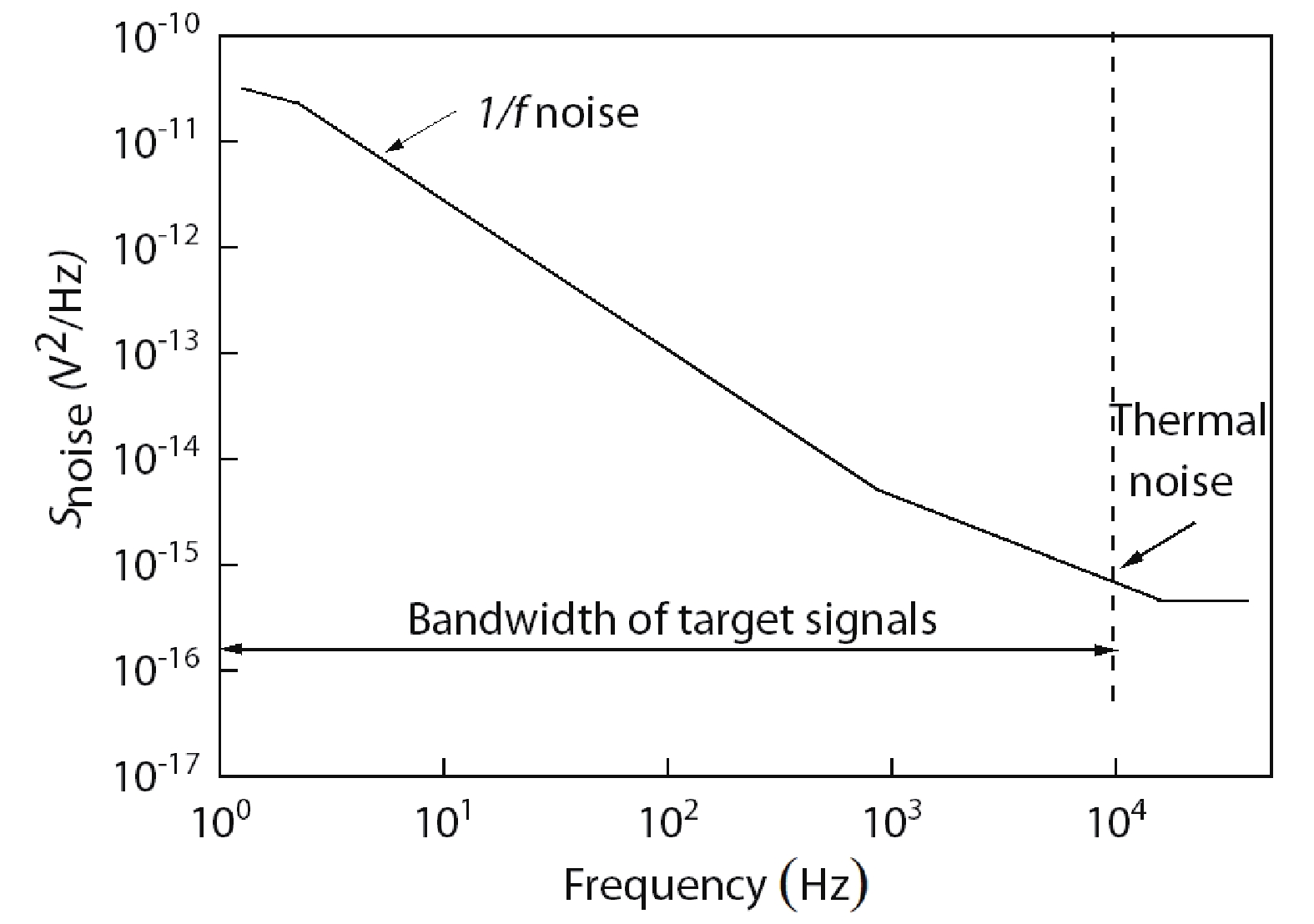
![]()
Figure 1.Schematic diagram of the noise power spectral density of VHDs.
To effectively remove the offset and 1/f noise of Hall devices, the dynamic offset cancellation technique has been broadly adopted[
In our work, a magnetic sensor microsystem integrated with a VHD has been implemented in a 0.18 μm low-voltage CMOS technology. The structure of an FSVHD is optimized for sensitivity improvement and noise reduction. A new four-phase SC circuit and its corresponding modulated circuit are proposed to effectively cancel Hall offset and linearly amplify the Hall signal. The experimental results show that the vertical Hall microsystem can achieve high system sensitivity, low residual offset, and high linearity, indicating that it is very suitable for a low-cost 2D or 3D Hall sensor microsystem.
2. Hall microsystem design
The block diagram of the proposed vertical Hall sensor is depicted in Fig. 2, which consists of a vertical Hall device, a spinning current (SC) switch box, an instrumentation amplifier (INA), a correlated double sampling (CDS) circuit, a sample/hold (S/H) adder, a low-pass filter (LPF), and a clock generator. The operating principle of the front-end Hall microsystem is described as follows. Firstly, the output Hall signals of the VHD are modulated to high frequency under the control of the four-phase SC switches. Then, the differential Hall signals proportional to the changing magnetic field are amplified by the instrumentation amplifier. After that, the CDS and S/H adder cancel the offset and 1/f noise of the VHD and demodulate the Hall signal back to the low frequency at the same time. Finally, the low pass filter removes high-frequency harmonic components and outputs Hall signals with the low residual offset.
![]()
Figure 2.The block diagram of the proposed vertical Hall sensor.
2.1. Vertical Hall device
The optimization of the VHDs is based on a fully symmetric topology[
![]()
Figure 3.Schematic of (a) the FSVHD consisting of four interconnected 3CVHEs and (b) the four operating modes in the four-phase spinning technique.
A two-dimensional device simulation of the FSVHD has been implemented in 0.18-μm standard CMOS technology utilizing the Silvaco Atlas tool. Appropriate models, such as the magnetic model, Shockley–Read–Hall recombination, low-field mobility, etc., are applied in the TCAD simulation. Firstly, the influence of the width (Ln) of the central N+ contacts on the sensitivity was simulated at the fixed distance (Ld) between the central and the two side N+ contacts. Fig. 4(a) compares the voltage-related sensitivity of the FSVHD as a function of bias voltage for three different sizes of Ln when a magnetic field of 0.1 T is applied. It is found that at the bias of 2 V, the sensitivity is reduced from 0.9 %/T to 0.68 %/T when the width of Ln is increased from 0.42 to 0.8 μm. This is because for the central N+ sense contact, the smaller the width, the higher the geometry factor, leading to the larger sensitivity. Limited by the design rule of the 0.18 μm CMOS technology, the minimum width of the central N+ implantation is only allowed to be 0.42 μm, thus, it is designed to be 0.42 μm for maximum sensitivity. Secondly, the distance (Ld) is changed from 0.8 to 2.1 μm to investigate the variation of the sensitivity when the width of Ln is fixed at 0.42 μm. Fig. 4(b) shows the voltage-related sensitivity as a function of bias voltage at three different distances of Ld. It is seen that the shorter Ld leads to higher sensitivity, which is due to the reduction of the short circuit effect of the FSVHDs. Consequently, the central N+ contacts need to be as close to the two side N+ contacts as possible. However, the shorter distance Ld will lead to a larger offset. Considering the offset limit, the distance Ld is selected to 1.5 μm, not the minimum size.
![]()
Figure 4.(Color online) TCAD simulation results for the FSVHD sensitivity. Sensitivity as a function of (a)
2.2. Four-phase spinning current switches
To better eliminate the offset and 1/f noise of the FSVHD, a novel four-phase SC circuit that consists of 16 NMOS switches is proposed in Fig. 5(a). The SC circuit is based on the periodic interchangeability of the biasing and sensing terminals of the FSVHD under the control of four-phase sequential clocks, enabling the polarity change of Hall voltage and offset, as depicted in Fig. 5(b). When clk1 and clk2 go high successively, the polarity of the output Hall voltage changes periodically, while the polarity of the offset voltage remains unchanged[
![]()
Figure 5.Schematic diagram of (a) the switched vertical Hall device using four-phase spinning current operation and (b) the output Hall voltage and offset voltage corresponding to the four-phase sequence clocks.
where the VH and VOP are the Hall and offset voltages of the FSVHD, respectively.
Similarly, when clk3 and clk4 turn high in the order, the FSVHD is operated in the second two-phase SC stage. The polarity change of the output Hall voltage is the same as that in the first two-phase SC stage. Note that the polarity of the offset voltage is not changed in the second two-phase SC, but it is the opposite of the first two-phase SC. The output voltage can be expressed as
It can be seen that after the four-phase SC modulation, the output Hall voltage can be distinguished from the offset voltage, which facilitates subsequent dynamic offset elimination.
2.3. Signal conditioner
After four-phase SC modulation, the mixing signals including Hall and offset voltages are input into the instrumentation amplifier for magnitude amplification. Fig. 6 schematically shows the bridge instrumentation amplifier configuration with resistive voltage feedback and three same two-stage operational amplifiers (op-amps). Among them, the op-amp adopts a two-stage amplifier with a PMOS differential input pair, which enables the circuit to work normally at a lower common-mode level, and it also has a high ability to suppress common-mode interference signals.
![]()
Figure 6.The schematic diagram of the bridge instrumentation amplifier.
The amplified signals are then demodulated by the correlated double sampling (CDS) circuit, the S/H, and the adder, as shown in Fig. 7. The inset of Fig. 5(b) schematically shows the output waveform of the CDS circuit. When the clk5 and clk6 are high, respectively, the mixed input signals corresponding to the first and the second SC stages are sampled twice, and then we can obtain the CDS output voltage that equals the second sampling value minus the first sampling value:
![]()
Figure 7.The schematic diagram of the CDS demodulation circuit.
where the Au denotes the total voltage gain of the front-end vertical Hall sensor, and ΔVOP,12= Au(VOP1– VOP2).
In the same way, when the input signals corresponding to the third and fourth SC stages are sampled by the CDS circuit, we can also obtain:
where ΔVOP,34= Au(VOP4– VOP3).
Next, under the control of the clk7 and clk8, the output signals of the CDS circuit are sampled and maintained by two S/H circuits. The output voltages of the CDS are fed into the adder to obtain the final Hall output voltage:
Here, ΔVOP= Au(VOP1– VOP2– VOP3 + VOP4), which determines the residual offset of the Hall sensor.
Since the offset voltages from two S/H circuits have the opposite polarity, the offset and 1/f noise can be further eliminated by the add operation. Finally, a low residual offset is obtainable, meanwhile, the spectrum of the Hall signal is demodulated back to the baseband.
3. Measurement results and discussions
The prototype of the proposed vertical Hall sensor was fabricated in a low-voltage 0.18 μm 2-poly 6-metal CMOS technology. Fig. 8 displays the micrographs of the sensor chip, which occupies 1.24 × 1.24 mm2, including the I/O pads and coupling capacitors.
![]()
Figure 8.(Color online) Hall sensor microphotograph: whole chip including pads with an active area with the back-annotated layout of main circuital blocks.
The performance of the vertical Hall sensor was measured by applying a magnetic field parallel to the chip. Fig. 9 shows the experimental setup for the sensor microsystem, which consists of a Gauss meter, a high-precision nano voltmeter, a semiconductor parameter analyzer, a magnetic field generator, and a power supply. The linear magnetic field is produced by a magnetic field generator driven by a power supply. After bonding, the vertical Hall devices and sensor chip were placed in the center of the magnetic field generator where the magnetic field intensity was calibrated by a Gaussian meter. Firstly, the offset voltage and the noise power spectral density of FSVHDs were tested without applying a magnetic field. Then, the Hall voltage of FSVHDs was measured in the magnetic field range from 0 to 200 mT by adjusting the output current of the power supply. Here, the Hall voltage including offset was tested by the high-precision nano voltmeter, and the noise of the FSVHD was characterized by the FS-PRO semiconductor parameter analyzer. Finally, the front-end vertical Hall microsystem response to a magnetic field was measured. The four-phase sequential clocks and the CDS sampling clocks required for the vertical Hall sensor chip were provided by an external FPGA development board. Under the control of the four-phase sequential clocks, the four-phase SC box outputs modulated signals, including Hall, and offset voltages with different polarities. After the mixed signals are amplified by the instrumentation amplifier, they are sampled during the second and fourth SC stages by the CDS demodulated circuit, respectively, and then the two sampled voltages are summed by the adder. As a result, the Hall voltage is demodulated back to the low-frequency signal, meanwhile, the offset and 1/f noise are dynamically removed and a low residual offset can be achieved.
![]()
Figure 9.(Color online) Experimental setup.
Fig. 10 illustrates the output Hall voltage of the optimized FSVHD (Ln = 0.42 μm and Ld =1.5 μm) as a function of the magnetic field at a bias of 2 V. It is found that the output Hall voltage is linearly increased with the magnetic field intensity in the range from 0 to 100 mT. At the magnetic field of 100 mT, the measured Hall voltage of the optimized FSVHD is about 1.415 mV, thus the voltage-related sensitivity is calculated as 0.71 %/T. By comparison, the initial FSVHD without optimization with a larger size (Ln2 = 0.6 μm and Ld = 2.89 μm) has a lower sensitivity of 0.46 %/T. It is indicated that the miniaturization of the device is very helpful to improve the sensitivity of the FSVHD.
![]()
Figure 10.(Color online) Test Hall voltages as a function of in-plane magnetic field for two FSVHDs. The inset picture shows the voltage-related sensitivity of two FSVHDs.
Fig. 11(a) illustrates the offset of the optimized FSVHDs operated at the four-phase spinning current modes. It is found that the offset voltages increase with the bias voltage. The offset voltages at mode 1 and mode 3 are electronically symmetrical. Similarly, modes 2 and 4 also have symmetrical offset voltages. At the bias of 2 V, the absolute value of the initial offset is about 3 mV, but the mean offset is only 15 μV for the four modes. Therefore, the four-phase SC technique can effectively eliminate the offset of the FSVHD. The measurement results of the noise power spectrum are illustrated in Fig. 11(b). The presented FSVHD shows dominating 1/f noise at low frequencies. It is observed that the 1/f noise level is increased with the bias voltage and the corner frequency quickly shifts to higher values. At the bias of 0.6 V, the corner frequency is about 100 kHz. As the bias is increased to 2 V, it is moved to about 1 MHz. In fact, at the 1 MHz corner frequency, the 1/f noise is reduced to a small level of 2 nV/
![]()
Figure 11.(Color online) Tested results of the optimized FSVHD. (a) Offset as a function of bias voltage and (b) 1/
Fig.12 shows the output Hall voltage versus magnetic field amplitude for the front-end vertical Hall sensor chip. The Hall output voltage is linearly increased with the magnetic field. The linearity reaches 99.9% in the magnetic field range from –200 to 200 mT and the sensor system sensitivity was determined to be 1.22 V/T. Thanks to the application of the four-phase SC modulation and a CDS demodulation technique, a low residual offset of 60 μT is obtained. In contrast, the residual offset is larger than 200 μT in the vertical Hall sensor using the conventional two-phase SC technique. Additionally, the 1/f noise at low frequency is also reduced by a factor of 5 compared with the vertical Hall sensor without the application of the four-phase SC method.
![]()
Figure 12.(Color online) Measured differential output voltages of the vertical Hall sensor as a function of a magnetic field.
Table 1 summarizes the principal characteristics of this work compared to the state of the art[
4. Conclusions
A front-end CMOS vertical Hall sensor microsystem fabricated in a low-voltage 0.18
Acknowledgements
This work was supported by the National Natural Science Foundation of China (Nos. 61871231, 62171233) and the Natural Science Foundation of Jiangsu Province, China (No. BK20181390), and the Key Research & Development Plan of Jiangsu Province, China (No. BE2019741), and the Agricultural Science and Technology Independent Innovation Foundation of Jiangsu Province, China (No. CX(21)3062).
References
[1] M Banjevic, B Furrer, M Blagojevic et al. High-speed CMOS magnetic angle sensor based on miniaturized circular vertical Hall devices. Sens Actuators A, 178, 64(2012).
[2] A Ajbl, M Pastre, M Kayal. A fully integrated Hall sensor microsystem for contactless current measurement. IEEE Sens J, 13, 2271(2013).
[3] Y Xu, H B Pan, S Z He et al. Monolithic H-bridge brushless DC vibration motor driver with a highly sensitive Hall sensor in 0.18 μm complementary metal-oxide semiconductor technology. IET Circuits Devices Syst, 7, 204(2013).
[4] S Paliwal, S Yenuganti. A differential Hall effect based pressure sensor. J Electr Eng Technol, 16, 1119(2021).
[5] Y Xu, X Hu, L Jiang. An analytical geometry optimization model for current-mode cross-like Hall plates. Sensors, 19, 2490(2019).
[6] H Huang, D Wang, W Li et al. A simplified compact model of miniaturized cross-shaped CMOS integrated Hall devices. J Semicond, 33, 084005(2012).
[7] J B Schell, J B Kammerer, L Hébrard et al. CMOS 3D Hall probe for magnetic field measurement in MRI scanner. IEEE 10th International New Circuits and Systems Conference (NEWCAS), 517(2012).
[8] S Wouters, V Vrankovi, C Rössler et al. Design and fabrication of an innovative three-axis Hall sensor. Sens Actuators A, 237, 62(2017).
[9] C Wouters, V Vranković, P Chevtsov et al. Calibration scheme for a new type of 3D Hall sensor. Sens Actuators A, 257, 38(2017).
[10] O Paul, R Raz, T Kaufmann. Analysis of the offset of semiconductor vertical Hall devices. Sens Actuators A, 174, 24(2012).
[11] J Pascal, L Hébrard, J B Kammerer et al. First vertical Hall device in standard 0.35 μm CMOS technology. Sens Actuators A, 147, 41(2008).
[12] J Pascal, L Hébrard, V Frick et al. Intrinsic limits of the sensitivity of CMOS integrated vertical Hall devices. Sens Actuators A, 152, 21(2009).
[13] E Schurig, M Demierre, C Schott et al. A vertical Hall device in CMOS high-voltage technology. Sens Actuators A, 97/98, 47(2002).
[14] E Schurig, C Schott, P A Besse et al. 0.2 mT residual offset of CMOS integrated vertical Hall sensors. Sens Actuators A, 110, 98(2004).
[15] G M Sung, W Y Wang, C P Yu. Analysis and modeling of one-dimensional folded vertical Hall sensor with readout circuit. IEEE Sens J, 17, 6880(2017).
[16] H Heidari, E Bonizzoni, U Gatti et al. CMOS vertical Hall magnetic sensors on flexible substrate. IEEE Sens J, 16, 9736(2016).
[17] C Sander, M C Vecchi, M Cornils et al. From three contact vertical Hall elements to symmetrized vertical Hall sensors with low offset. Sens Actuators A, 240, 92(2016).
[18] C Sander, C Leube, O Paul. Compact two-dimensional CMOS Hall sensor based on switchable configurations of four three-contact elements. Sens Actuators A, 248, 281(2016).
[19] G Bilotti, R A. Monolithic magnetic Hall sensor using dynamic quadrature offset cancellation. IEEE J Solid-State Circuits, 32, 829(1997).
[20] Z B Randjelovic, M Kayal, R Popovic et al. Highly sensitive Hall magnetic sensor microsystem in CMOS technology. IEEE J Solid-State Circuits, 37, 151(2002).
[21] Y Xu, H B Pan, S Z He et al. A highly sensitive CMOS digital Hall sensor for low magnetic field applications. Sensors, 12, 2162(2012).
[22] J Jiang, W J Kindt, K A Makinwa. A continuous-time ripple reduction technique for spinning-current Hall sensors. IEEE J Solid-State Circuits, 49, 1525(2014).
[23] M Crescentini, M Marchesi, A Romani et al. A broadband, on-chip sensor based on Hall effect for current measurements in smart power circuits. IEEE Trans Instrum Meas, 67, 1470(2018).
[24] L Osberger, V Frick, L Hébrard. High resolution shallow vertical Hall sensor operated with four-phase bi-current spinning current. Sens Actuators A, 244, 270(2016).
[25] A Girgin, M Bilmez, H Y Amin et al. A silicon Hall sensor SoC for current sensors. Microelectron J, 90, 12(2019).
[26] H Heidari, E Bonizzoni, U Gatti, F Maloberti. A CMOS current-mode magnetic Hall sensor with integrated front-end. IEEE Trans Circuits Syst I, 62, 1270(2015).

Set citation alerts for the article
Please enter your email address
© Copyright 2018-2021 | Chinese Laser Press. All Rights Reserved 沪ICP备15018463号-20