Yutong Zhang, Zhuoya Zhu, Shuai Zhang, Xianxin Wu, Wenna Du, Xinfeng Liu. Spectroscopy and carrier dynamics of one-dimensional nanostructures[J]. Journal of Semiconductors, 2022, 43(12): 121201
Search by keywords or author
- Journal of Semiconductors
- Vol. 43, Issue 12, 121201 (2022)
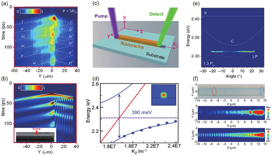
![(Color online) (a) Time-resolved spatial distribution of the polariton emission at 5Pth in a wire withδ = –3 meV[24]. (b) Simulation considering polariton condensates propagating and interacting with the excitonic reservoir. The excitation spot is located 35μm from the right edge of the wire (inset)[24]. (c) Schematic of experimental setup. One laser excites at one facet of wire and wave-guide emission collected at another facet of the same wire[15]. (d) Dispersion curves of MAPbBr3 wires with width × length dimensions of 0.32 × 3.66µm2[15,45]. (e) Polariton dispersion at 1.3Pth, showing symmetric dominant emission at around ±20°[70]. (f) Schematic of pumping spot and collection spot on the microwire microcavity and measured and simulated real-space images of the microwire microcavity above the polariton condensation threshold, respectively[70].](/richHtml/jos/2022/43/12/121201/jos_43_12_121201_f1.jpg)
Fig. 1. (Color online) (a) Time-resolved spatial distribution of the polariton emission at 5Pth in a wire withδ = –3 meV[24]. (b) Simulation considering polariton condensates propagating and interacting with the excitonic reservoir. The excitation spot is located 35μm from the right edge of the wire (inset)[24]. (c) Schematic of experimental setup. One laser excites at one facet of wire and wave-guide emission collected at another facet of the same wire[15]. (d) Dispersion curves of MAPbBr3 wires with width × length dimensions of 0.32 × 3.66µm2[15,45]. (e) Polariton dispersion at 1.3Pth, showing symmetric dominant emission at around ±20°[70]. (f) Schematic of pumping spot and collection spot on the microwire microcavity and measured and simulated real-space images of the microwire microcavity above the polariton condensation threshold, respectively[70].
![(Color online) (a) Geometric representation of 1D multi-layered GaAs/AlAs based photonic crystal having Fibonacci sequence[73]. (b) Transmission spectra of GaAs/AlAs based one dimensional multilayered quasiperiodic photonic crystal having variation in layer thickness of GaAs (dg)[73]. (c) Transmission spectra of GaAs/AlAs based one dimensional multilayered quasiperiodic photonic crystal having variation in layer thickness of AlAs (da)[73]. (d) Schematic diagram of the femtosecond laser micromachining set-up used for the fabrication of 1D PC channel waveguides[74]. (e) Optical microscope images (top view) of the propagating streak at 632.8 nm and semi-log plots showing the exponentially decaying intensity along the propagation direction for waveguides of different widths for vertical and horizontal input polarizations[74].](/richHtml/jos/2022/43/12/121201/jos_43_12_121201_f2.jpg)
Fig. 2. (Color online) (a) Geometric representation of 1D multi-layered GaAs/AlAs based photonic crystal having Fibonacci sequence[73]. (b) Transmission spectra of GaAs/AlAs based one dimensional multilayered quasiperiodic photonic crystal having variation in layer thickness of GaAs (dg)[73]. (c) Transmission spectra of GaAs/AlAs based one dimensional multilayered quasiperiodic photonic crystal having variation in layer thickness of AlAs (da)[73]. (d) Schematic diagram of the femtosecond laser micromachining set-up used for the fabrication of 1D PC channel waveguides[74]. (e) Optical microscope images (top view) of the propagating streak at 632.8 nm and semi-log plots showing the exponentially decaying intensity along the propagation direction for waveguides of different widths for vertical and horizontal input polarizations[74].
Fig. 3. (Color online) (a) Hybrid device configuration (on the top). The insets highlight the metal slotted structure[83]. (b)Q-factor and (c) mode volume as a function of the gapG and the slot widths[83]. (d) Layout of the experiment and the PC/OLED structure with two metal nanolayers[84]. (e) Electroluminescence spectrum from the 1D PC with the super yellow (SY) light-emitting layer, which is sandwiched between two metal nanolayers. The standard SY emission spectrum is presented as a cyan curve for comparison[84]. (f) Superimposed experimental spectra (as smoothed contour lines) and the integral of the optical electric field in the SY light-emitting layer[84].
Fig. 4. (Color online) Schematic of the one-dimensional SSH model.
Fig. 5. (Color online) (a) Scanning electron microscopy image of the zigzag chain on perovskite layer before the deposition of top DBR. The white dashed circles are added for visibility.t andt′ represent the intracell and intercell hopping strengths. Scale bar, 1μm[88]. (b) Schematic of a topological laser array made of nine micro-ring resonators with alternating weak (t1) and strong (t2) couplings, emulating an SSH model. A layer of 10-nm Cr (shown in yellow) is deposited on top of every second element to introduce distributed gain and loss. The red halos represent the intensity profile of the oscillating zero mode that resides at the central site and decays exponentially away from the center, with zero intensity in every second element[93]. (c) Energy-resolved momentum-space polariton dispersion at 0.5Pth in Y polarization. The white dashed lines highlight the topological gap with topological polariton edge states inside thes band[88]. (d) Energy-resolved momentum-space polariton dispersion at 2.0Pth in Y polarization. Real-space images of higher energy state and the topological edge states at 2.0Pth (inset)[88]. (e) Schematic of the nanocavity formed by interfacing two photonic crystals (PCs) with a common bandgap and distinct Zak phases[95]. (f) Single-super mode lasing from the topological micro-laser under the pumping condition. Lasing mode profile of the topological micro laser (inset)[93]. (g) Position-dependent PL intensities measured for the topological nanocavities with differentd1 values[95].

Set citation alerts for the article
Please enter your email address


