1CAS Key Laboratory of Standardization and Measurement for Nanotechnology, CAS Center for Excellence in Nanoscience, National Center for Nanoscience and Technology, Beijing 100190, China
2University of Chinese Academy of Sciences, Beijing 100049, China
In recent years, one-dimensional (1D) nanomaterials have raised researcher's interest because of their unique structural characteristic to generate and confine the optical signal and their promising prospects in photonic applications. In this review, we summarized the recent research advances on the spectroscopy and carrier dynamics of 1D nanostructures. First, the condensation and propagation of exciton–polaritons in nanowires (NWs) are introduced. Second, we discussed the properties of 1D photonic crystal (PC) and applications in photonic–plasmonic structures. Third, the observation of topological edge states in 1D topological structures is introduced. Finally, the perspective on the potential opportunities and remaining challenges of 1D nanomaterials is proposed.In recent years, one-dimensional (1D) nanomaterials have raised researcher's interest because of their unique structural characteristic to generate and confine the optical signal and their promising prospects in photonic applications. In this review, we summarized the recent research advances on the spectroscopy and carrier dynamics of 1D nanostructures. First, the condensation and propagation of exciton–polaritons in nanowires (NWs) are introduced. Second, we discussed the properties of 1D photonic crystal (PC) and applications in photonic–plasmonic structures. Third, the observation of topological edge states in 1D topological structures is introduced. Finally, the perspective on the potential opportunities and remaining challenges of 1D nanomaterials is proposed.
Introduction
Nanostructured materials are defined as having at least 1D in the range of 1–100 nm in the three-dimensional spatial range. When the size of a material is reduced to the nanoscale, the number of surface atoms is limited to a specific ratio, and exhibit striking changes in their physical and chemical properties. The properties of nanoscale materials include quantum tunneling effects, quantum size effects and Coulomb blocking, and thus make them behave differently from their bulk counterparts.
Nanomaterials can be classified as zero-dimensional (0D), one-dimensional (1D), two-dimensional (2D) and three-dimensional (3D) by dimensionality. 0D nanomaterials are also called quantum dots. Their size is reduced to the nanometer scale in all three dimensions, the restricted electron motion leads to a discrete atom-like electronic structure and size-dependent energy levels[1]. This enables the design of nanomaterials with widely tunable light absorption, narrow linewidth[2] and significant nonlinear optical effect[3] leading to its potential advantages in microelectronics and optoelectronic devices[4]. 2D nanomaterials represent sheet-like nanostructures with the lateral size larger than 100 nm but the thickness is only a few nanometers or few-atoms thick[5]. Graphene, hexagonal boron nitride (h-BN)[6,7] and transition metal dichalcogenides (TMDs)[8-10] are typical 2D nanomaterials that exhibit versatile properties including ultrahigh specific surface area and high carrier mobility[11]. 3D nanomaterials refer to materials with nanoscale features in three dimensions, and are spatial organizations constructed using 0D, 1D and 2D nanostructures. 3D nanostructures can exhibit novel electronic and optical properties as a result of interactions and coupling between the excitons, magnetic moments which could differ from those properties of the individual nanoscale units[12,13]. Various 3D nanostructures have been reported for sustainable energy conversion and optical applications[14]. Among these, 1D nanomaterial, such as ZnO NWs, III–V NWs, and so on, can range in diameter from a few nanometers to a few hundred nanometers, while the length is not limited to tens of microns. 1D nanomaterials have stimulated intense interest in recent years due to their importance in fundamental physical research and in potential technological applications, such as the underlying physics of light−matter interactions in 1D nanomaterial[15,16], the physical mechanism of light emission and the carrier dynamics from NW heterostructures[17,18], photodetectors[19], lasers and field-effect transistors[20-22].
1D semiconductor nanomaterials have unique advantages over traditional semiconductor materials. As wire-like nanomaterials, 1D semiconductor nanomaterials can propagate electrons, photons, excitons, and so on[23-26]. In their axes, they can be used not only as the "building blocks" of functional semiconductor devices, but also as optical or electrical leads in integrated devices[27-29]. In 2020, Shanget al. prepared single crystal NWs by chemical vapor deposition (CVD) and investigate the light propagation behavior at room temperature by spatially resolved photoluminescence spectroscopy[30]. They demonstrated that the light propagates as exciton–polariton and exhibits significant spatial dispersion at room temperature. The reduction of dimension increases exciton−photon coupling and the exciton fraction, increasing the light absorption coefficient and group index 5- and 3-fold, respectively, relative to those of bulk films and slowing the light group velocity by ~74%. Besides, the chemical composition and structure of semiconductor nanomaterials can be very complex. By varying the preparation process, 1D semiconductor nanomaterials of various compositions can be obtained, and they can also be prepared as axial heterojunctions or radial heterostructures in the form of core-shells and heterostructures with gradients in chemical composition in the axial direction[31]. Jacopinet al. reported the diffusion of carriers in graded InGaN/GaN quantum wells in a NW by the time-resolved cathodo-luminescence[32]. They concluded that this diffusion process was thermally activated by probing the local dynamics at the nanoscale between 4 and 250 K, and the carrier motion was isotropic and does not follow the indium gradient. Hoet al. prepared the CsPbBr3/MoO3 core–shell NWs in 2020[33], and they demonstrated that a highly increase in the field-effect hole mobility from 1.5 to 23.3 cm2/(V·s) was accomplished after depositing the 10 nm thick MoO3 shell because of the efficient interfacial charge transfer and reduced impurity scattering. In addition, the MoO3 shell can provide excellent surface passivation to the CsPbBr3 NW core and improve the air stability of CsPbBr3/MoO3 core–shell NW devices.
Most information technologies are based on the fast response of small size and high-speed microelectronic devices. The fundamental study of carrier dynamics occurring on the picosecond or even femtosecond time scale provides guidance for the design and preparation of high-speed devices. In this review, we focus on the latest research progress on the spectroscopy and carrier dynamics of 1D structures. In Section 2, we review the condensation and propagation of exciton–polariton in NWs. In Section 3, we discuss the basic properties of 1D PC and applications in photonic-plasmonic structures. In Section 4, the edge-state observation of 1D topological structures is briefly introduced. Finally, we will finish with a summary and an outlook on how we believe the field will develop further in the coming years.
Spectroscopy and carrier dynamics of nanowires
NWs fabricated from many material systems have been studied, such as zinc oxide (ZnO), III–V. Recently hybrid perovskites have gained widespread attention with the refinement of NW synthesis methods[34-36]. In particular, NW growth methods, available substrates and source materials are more diverse than those for crystalline epitaxial growth[37-39]. Inexpensive and simple vapor-liquid-solid (VLS) methods have led to a dramatic increase in NW research over the past 20 years[40-43].
Exciton–polaritons are quasi-particles of half-light and half-matter formed by quantum superposition of electron–hole pairs (excitons) and confined cavity photons; therefore, exciton–polaritons have both the strong nonlinear effects of the exciton part and the low effective mass of the photon part[44]. Besides, exciton–polaritons show large overlap and strong lateral confinement between photon modes and excitons in 1D cavities, resulting in large Rabi-splitting[45]. Exciton–polaritons promote the realization of slow light, low threshold polaritons laser and other applications[46-51]. In addition, its quantum fluid properties provide the possibility for the occurrence of special phenomena such as Bose-Einstein condensation[52-56], super-fluid[57-60] and vortex[61-64].
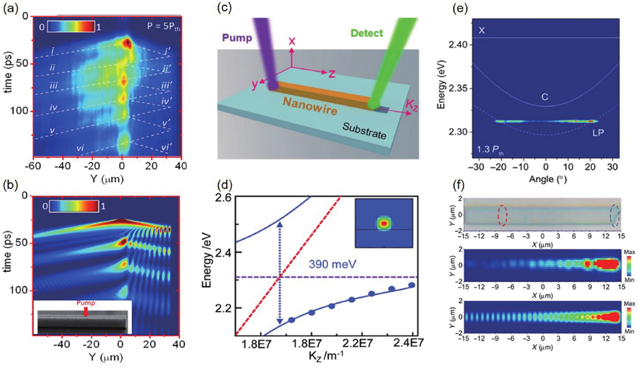
In 2012, Blochet al. investigated the dynamics of propagating polariton condensates in 1D microcavities through time resolved experiments[24]. GaAs wire cavities with a high-quality factor (Q ~ 36 000) were fabricated using electron beam lithography and reactive ion etching. As shown inFig. 1(a), the authors placed the excitation spot 35μm away from one of the edges of the wire. Above threshold (5Pth), the condensate is formed after the arrival of the excitation pulse. Two condensates are ejected from the excitation region, one departing to the left [labeled (i)] and another one to the right [labeled (i’)]. When condensate i’ reaches the edge of the wire, it is reflected and propagates back and a strong increase of the emission signal is observed when it gets back to the pumped area. Enhancement of the emission signal takes place five times in the observation window. Considering polariton condensates propagating and interacting with the excitonic reservoir, the simulation is shown inFig. 1(b). The authors measured amplification gain at each of the successive repopulations of the condensate, showing a gain of more than 4, and a time decay of the gain on the order of 300 ps. The two key factors in achieving the propagation of exciton-polaritons condensates over macroscopic distances are propagation with controlled velocity and polariton amplification through the nonresonantly excited area. The presence of an uncondensed excitonic reservoir in the excitation region induces exciton–polariton repulsive interactions. The reservoir induces an interaction energy that can be transformed into kinetic energy when the condensate exits the excitation region, resulting in the acceleration and propagation of the polariton condensate on both sides of this region. Once the condensate exits the excitation spot, the propagation velocity remains constant and can be directly measured from the slope of the polariton trajectory in the real space-time resolved images. The group velocity is inversely proportional to the square root of the polariton mass, which is fixed by the curvature of the polariton dispersion. By varying the degree of detuning and thus the curvature, they can control the group velocity of the expelled polariton packet. This polariton amplification opens new avenues for application of the cascaded polariton function and accelerates researches in optical transistor under non-resonant pumping.
Figure 1.(Color online) (a) Time-resolved spatial distribution of the polariton emission at 5Pth in a wire withδ = –3 meV[24]. (b) Simulation considering polariton condensates propagating and interacting with the excitonic reservoir. The excitation spot is located 35μm from the right edge of the wire (inset)[24]. (c) Schematic of experimental setup. One laser excites at one facet of wire and wave-guide emission collected at another facet of the same wire[15]. (d) Dispersion curves of MAPbBr3 wires with width × length dimensions of 0.32 × 3.66µm2[15,45]. (e) Polariton dispersion at 1.3Pth, showing symmetric dominant emission at around ±20°[70]. (f) Schematic of pumping spot and collection spot on the microwire microcavity and measured and simulated real-space images of the microwire microcavity above the polariton condensation threshold, respectively[70].
Halide perovskites are expected to be the basic materials for a new generation of optoelectronic devices due to their high defect tolerance and long photocarrier lifetime[35,65]. Owing to a unique ease of fabrication and richness of tunability, halide perovskites have become an excellent system for room-temperature polaritons[45,66-68]. In 2018, Zhanget al. presented the strong exciton–photon coupling in hybrid inorganic–organic MAPbBr3 micro/nanowire cavities at room temperature[15]. A schematic of experimental setup is shown inFig. 1(c). Continuous wave (CW) 405 nm laser is focused to excite edge of perovskite wire. Then PL is generated and propagates along the wire and the emission from the other end is collected in the reflective configuration. Energy (E) versus wavevector (k) dispersion is investigated to detect the exciton–polariton effects in MAPbBr3 micro/nanowire with different effective mode volumes (Veff). Experimental and theoretical results showed larger Rabi splitting energy in smaller diameter wire and the Rabi splitting energy increases from 268 meV (for bulk polariton) to 390 meV with the decrease of theVeff of the nanowires (Fig. 1(d)). Besides, they demonstrated that the photonic lasing is generated instead of the polariton lasing due to the decrease of the oscillator strength and the weakening of the exciton–photon coupling strength owing to the carrier screening effect with increasing pump fluence. The carrier screening effect with increasing pump fluence weakens the interaction between electrons and holes, and fewer and fewer free states are available to build the two-particle wavefunction of the exciton. The carrier screening effect eventually gives rise to a decrease in the oscillator strength and thus a decrease in Rabi-splitting energy
: at high pumping powers there is a gradual loss of coupling strength between the exciton and photons. Eventually, when the carrier shielding effect is strong enough, no excitons can exist in the system anymore, and so no polaritons as well[69]. The room temperature exciton–polaritons makes MAPbBr3 micro/nanowire an excellent polariton material and broadens the application of perovskite materials in polariton-based devices filed. Suet al. demonstrated that the first experimental realization of coherent polariton condensate flow at room temperature in a 1D all-inorganic CsPbBr3 perovskite quantum wire microcavity by a nonresonant excitation[70]. The polariton behavior of CsPbBr3 microcavity at room temperature was studied by angle-resolved photoluminescence spectroscopy. With the pump power density reaches to 1.3Pth, polariton condensates at around ±20° of emission angle as shown inFig. 1(e). With the pumping of the system, the polariton condensate acquires a nonzero in-plane wave vector because of polariton-exciton repulsive interactions. Thus, polariton condensates can propagate along the micro/nanowire. Since the propagating polariton condensate is not in the ground state of the system, it can be considered as a non-equilibrium coherent condensate, which still carries coherence from the condensation point. Experimental and theoretical results revealed that the polariton condensate exhibits high-speed propagation over macroscopic distances of 60 mm while still preserving the spontaneous spatial coherence (Fig. 1(f)). Their findings pave the way for the application of coherent polariton condensate flow in all-optical integrated logic circuits and polarized devices operating at room temperature.
Spectroscopy and carrier dynamics of 1D photonic crystals
Photonic crystals (PC) were first introduced in 1987 as an artificial periodic structure formed by the periodic arrangement of materials with different refractive indices in space[71]. 1D PCs are multi-layer structures formed by stacking materials or media with different refractive indices in a certain order, and their refractive indices show fixed periodic fluctuations in one direction. According to the electromagnetic field theory, the electromagnetic field in a medium with spatially periodic dielectric coefficient distribution follows the Maxwell equation:
where
is the average relative dielectric constant.
is the modulating part of the relative permittivity, which varies periodically with the spatial position.
is the speed of light in vacuum.
is the frequency and
is the electric field vector of the electromagnetic wave. By solving the equation, it can be found that the equation has a solution only at some specific frequencies, while the equation has no solution at some frequency ranges. In other words, some frequencies of electromagnetic waves in a dielectric structure with periodic dielectric constant distribution are forbidden. The special periodic structure of photonic crystals enables them to block the transmission of photons of specific wavelengths[71,72]. By designing the structure of PC, the photonic band can be artificially adjusted to achieve on-demand regulation of the light field distribution in PC devices.
In 2021, Biswalet al. investigated the optical behavior of GaAs/AlAs based 1D multi-layered quasi-periodic photonic crystal by employing the transfer matrix method and analyzed the transmission spectra of the crystal at the long-wave limit (Fig. 2(a))[73]. Various quasi-sequences (Fibonacci, Octonacci and Dodecanacci) along with the periodic structure are considered to get a clear bandgap for different generation number as shown inFigs. 2(b) and2(c). In addition, they observed that there is a reduction in both the bandgap and optical transmission peaks with a mirrored symmetry of transmittance within a frequency range, for both the quasi-periodic and periodic arrangement of multilayers while varying the thickness of the layer. The features of a multilayered quasi-system are very useful for designing new optical or electrical devices based on PC structures. In 2022, Lis et al. discussed 1D PC channel waveguides of different widths and waveguiding characteristics were studied in the end-fire coupling geometry[74]. The micrograph inFig. 2(d) shows the formation of multi-layered structure comprising of uniform SiO2 and TiO2 layers. Polarization dependent studies showed that the modes supported by 1D PC planar waveguide and channel waveguide maintain the input polarization state during propagation. The propagation losses of planar waveguide and channel waveguide are compared. The typical images are showed inFig. 2(e) for 1D PC planar waveguide, 17.8 ± 0.5μm wide and 15.3 ± 0.5μm wide channel waveguides. As the width of the channel waveguide decreases, the propagation loss decreases due to better plane constraints of the mode. The design of 1D PC planar and channels is attractive for the development of integrated optical applications while maintaining polarization.
Figure 2.(Color online) (a) Geometric representation of 1D multi-layered GaAs/AlAs based photonic crystal having Fibonacci sequence[73]. (b) Transmission spectra of GaAs/AlAs based one dimensional multilayered quasiperiodic photonic crystal having variation in layer thickness of GaAs (dg)[73]. (c) Transmission spectra of GaAs/AlAs based one dimensional multilayered quasiperiodic photonic crystal having variation in layer thickness of AlAs (da)[73]. (d) Schematic diagram of the femtosecond laser micromachining set-up used for the fabrication of 1D PC channel waveguides[74]. (e) Optical microscope images (top view) of the propagating streak at 632.8 nm and semi-log plots showing the exponentially decaying intensity along the propagation direction for waveguides of different widths for vertical and horizontal input polarizations[74].
Surface plasmon polaritons (SPP) is an electron sparse wave propagating along the metal surface generated by the interaction of freely vibrating electrons present on the metal surface and incident photons, and is a special electromagnetic mode that confines the electromagnetic field to a small area of the metal surface and resonantly enhances it[75]. Thus, SPP is widely used in nonlinear optics, such as Raman scattering, second harmonic generation (SHG) and plasmonic laser[76-78]. However, the generation of SPP on precious metals is usually accompanied by severe ohmic losses resulting in the propagation of SPP suffering from large attenuation at the metal-dielectric interface[79,80]. In the following, we discuss that periodic PC structure with highQ mass factor on metal surface can enhance the light-material interaction and reduce the propagation loss of SPP at the metal-PC interface[81,82].
In 2016, Conteducaet al. proposed a hybrid microcavity with a 1D PC dielectric cavity vertically coupled to a plasmonic slot[83]. The hybrid device configuration and the metal slotted structures are shown inFig. 3(a). Through designing the PC cavity and the metal slot, the hybrid structures have achieved an ultra-highQ/V ratio of 106 (λ/n)−3 and a remarkable resonance transmission (T = 47%) under coupling between the dielectric cavity and surface plasmon resonances. For the sake of increasing the resonance transmissionT and preserving an ultra-highQ/V ratio, the authors analyzed influences of gap G and slot width S on these parameters as shown inFigs. 3(b) and3(c). Their results indicated that the photonic-plasmonic cavity is suitable for biosensing and optical trapping of living matter at the nanoscale, such as proteins and DNA sections. Recently, Konopskyet al. reported long-range surface plasmons (LRSPs) on a duplex metal nanolayer[84]. In this work, a current injection-driven organic light-emitting diode (OLED) is sandwiched between two thin metal layers (Au and Al electrodes) and deposited on a 1D photonic crystal (PC) as shown inFig. 3(d). The electroluminescence spectrum from the 1D PC shows that the LRSP resonance is seen at λLRSP = 575 nm, while two local maxima at 527 and 630 nm correspond to the bandgap edges of the structure under study (Fig. 3(e)). In addition, the stack of 29 experimental spectra of electroluminescence taken at different angular parameters and the calculated integral of the optical electric field in the light-emitting layer are shown inFig. 3(f), with a good agreement between these two figures. The multilayer structure containing an OLED on top of a 1D PC is hoped to lay foundation for future electric pumping of surface plasmon amplification by stimulated emission of radiation (SPASERs).
Figure 3.(Color online) (a) Hybrid device configuration (on the top). The insets highlight the metal slotted structure[83]. (b)Q-factor and (c) mode volume as a function of the gapG and the slot widths[83]. (d) Layout of the experiment and the PC/OLED structure with two metal nanolayers[84]. (e) Electroluminescence spectrum from the 1D PC with the super yellow (SY) light-emitting layer, which is sandwiched between two metal nanolayers. The standard SY emission spectrum is presented as a cyan curve for comparison[84]. (f) Superimposed experimental spectra (as smoothed contour lines) and the integral of the optical electric field in the SY light-emitting layer[84].
Spectroscopy and carrier dynamics of 1D topological structures
In recent years, topological structures have been widely used in cold atoms[85], condensed matter[86], and acoustics[87]. The combination of topological and photonic systems is mutually beneficial. Photonic systems provide a platform for topological physics observation of new phenomena and topological structures provide a new physical concept for the development of efficient optoelectronic devices. Up to now, topological phenomena have been proposed and applied in different photonic systems, including microcavity polaritonic systems[88-90], coupled resonator optical waveguides[91-93], PCs[94-95] and plasmonic systems[96]. The topological phase regulation of 1D ordered structures is inseparable from the symmetry regulation, of which the most important or widely discussed is the chiral symmetry. The most representative model is the Su-Schrieffer-Heeger (SSH) model proposed by Suet al. in 1979. This model was originally introduced in an electronic context to describe fractionalized charges in polyacetylene, which appear in the presence of a dimerization defect[97].
This model has a simplified structure, but it is highly representative of the properties of topological quantum systems, and some other models can be mapped to the SSH model. In the SSH model (Fig. 4), the unit cell is composed of two sites, multiple unit cells form a 1D dimer lattice chain with lattice constant
. The intracell (v) and intercell (w) hopping amplitudes of the 1D dimer lattice chain can be adjusted[89]. In the momentum space, such a model is captured by a Hamiltonian:
Figure 4.(Color online) Schematic of the one-dimensional SSH model.
Two energy bands with energy gaps with a gap width of 2
are obtained by solving the equation. The Hamiltonian exhibits two topologically distinct phases associated with the two possible dimerizationsv \gtw andv \ltw. The different topology of these two phases is revealed by considering the winding
of phaseφ(k) across the Brillouin zone:
Although the value of
associated with either dimerization depends on the definition of the unit cell, in finite-size chains the choice is unambiguous because v is defined by the hopping amplitude between the first and second sites of the chain. Under this definition, thev \gtw andv \ltw dimerization exhibits respectively strong and weak coupling between the edge sites and the rest of the chain and correspond to the trivial (
= 0) and non-trivial (
= 1) topological phases. The main characteristic of topological non-trivial is that a topological phase transition occurs at the boundary between the chain and the vacuum, resulting in an edge state, which is manifested in the energy band by the appearance of an edge state in the energy gap[88].
In 2017, St-Jeanet al. reported lasing in topological edge states of a 1D SSH lattice of coupled semiconductor micropillars that contained multiple GaAs quantum wells sandwiched between two GaAlAs Bragg mirrors[89]. Under non-resonant optical pumping, they demonstrated that gain occurred in the topological states localized at the edges of the SSH lattice. Recently, Suet al. demonstrated an exciton–polariton topological insulator with polarization-dependent phases in a 1D perovskite lattice at room temperature, which is based on the SSH model by coupling the s-orbital type polariton modes with a zigzag chain of nanopillars (Fig. 5(a))[88]. They observed that the perovskite lattice exhibited a typical dispersion in Y polarization with edge states under low excitation power of 0.5Pth (Fig. 5(c)), while polaritons tended to condense into selected states with maximum gain under strong excitation power of 2.0Pth (Fig. 5(d)). In addition, they demonstrated that the topological robustness was protected by the topological gap in the presence of certain structural deformations and topological modes always appear in the middle of the topological gap and localize in the edges.
Figure 5.(Color online) (a) Scanning electron microscopy image of the zigzag chain on perovskite layer before the deposition of top DBR. The white dashed circles are added for visibility.t andt′ represent the intracell and intercell hopping strengths. Scale bar, 1μm[88]. (b) Schematic of a topological laser array made of nine micro-ring resonators with alternating weak (t1) and strong (t2) couplings, emulating an SSH model. A layer of 10-nm Cr (shown in yellow) is deposited on top of every second element to introduce distributed gain and loss. The red halos represent the intensity profile of the oscillating zero mode that resides at the central site and decays exponentially away from the center, with zero intensity in every second element[93]. (c) Energy-resolved momentum-space polariton dispersion at 0.5Pth in Y polarization. The white dashed lines highlight the topological gap with topological polariton edge states inside thes band[88]. (d) Energy-resolved momentum-space polariton dispersion at 2.0Pth in Y polarization. Real-space images of higher energy state and the topological edge states at 2.0Pth (inset)[88]. (e) Schematic of the nanocavity formed by interfacing two photonic crystals (PCs) with a common bandgap and distinct Zak phases[95]. (f) Single-super mode lasing from the topological micro-laser under the pumping condition. Lasing mode profile of the topological micro laser (inset)[93]. (g) Position-dependent PL intensities measured for the topological nanocavities with differentd1 values[95].
In addition to the 1D micropillars array, the topological structure composed of micro-rings or PC nanocavities can also achieve robust single-mode topological laser[91,92,95]. Intracellular coupling strengtht and intercellular coupling strengtht' are achieved by interleaved separation between adjacent rings. In 2018, Zhaoet al. presented a topologically robust single-mode hybrid silicon micro-laser (Fig. 5(b))[93]. Intracellular coupling strengtht and intercellular coupling strengtht' are achieved by interleaved separation between adjacent rings as shown inFig. 5(f). The zero-mode lasing in the topological array is highly reliable, despite the mode competition in each ring and between the rings. The lasing action of the topological zero mode is further validated by the measurement of the spatial lasing mode profile. Because the zero mode is topologically protected by the applied symmetries, the available data suggested that the demonstrated laser action is stable and immune to moderate perturbations and defects. Otaet al. reported a one-dimensional topological single-mode PC nanocavity and its applications in lasing[95]. They demonstrated that the 0D interface state can be formed between PC nanoparticles with different Zak phases. The single-mode topological laser with a high spontaneous emission coupling factor (β) of 0.03 and threshold of 46μW is realized with a small mode volume and a quality factor of 59 700. The design schematic of the topological PC nanobeam cavity is shown inFig. 5(e) and two airbridge PC nanobeams respectively colored in red and blue are interfaced at the cavity center. Different electric field distributions, mode volumes, andQ factors can be obtained by etching air holes in nanobeams with different widths and thicknesses.Fig. 5(g) shows the normalized peak intensities of the interface modes taken along thex direction. The three curves are of the nanocavities with differentd1 and clearly exhibit the mode sizes being dependent ond1. The case ofd1 = 0
andd1 = 0.23
respectively show the smallest and largest mode distribution, as expected from the simulations. The authors studied the pump power dependence of the topological edge state formed in nanocavities. For the low pump power PL spectrum, a sharp peak of the localized cavity mode is observed with broad background emission stemming. When the pump power increases to the threshold value of 46μW, the cavity mode emission grows sharply and dominates the spectrum. The light-in-light-out curve exhibits an intensity jump as an s-like shape, which is typical for lasers. Their results show that nanoscale topological photonic crystals have a very important development prospect for miniaturization of topological lasers. The most important benefit of topological design using photonic crystals is that theQ value and mode volume can be controlled systematically by changing the parameters of photonic crystals, while maintaining single-mode operation.
Summary and outlook
Over the past three decades, there has been substantial progress in the synthesis, processing and characterization of 1D semiconductor nanostructures (e.g., III–V elements and perovskites). Numerous findings have been made to show how structures and chemical compositions affect the properties of nanostructures to design nanostructures with new and enhanced properties and applications. 1D semiconductor nanostructures provide an ideal platform for novel technological applications, such as integrated optoelectronic and photonic devices, biosensors, and energy conversion and storage devices. However, beyond these achievements, many challenges still remain in 1D semiconductor nanostructures.
For semiconductor NWs, experimental studies on NWs have focused on static state measurements and the highest time resolution is on the order of picoseconds. The exploration of underlying dynamics of the related polariton condensation process is not sufficient owing to the short lifetime of polaritons at room temperature, which require experimental resolution on sub-picosecond or femtosecond timescales. Heterostructures are an important mean of regulating the electronic structure and properties of materials, and even the directional selection of material properties can be achieved. The exploration and design of more high-performance 1D heterostructure devices have been research hotspots. In addition, further studies are needed to control the size and growth of high-quality crystals of 1D nanomaterials. In practical applications, precise control of growth and enhancement of synthetic yield are also problems to be solved. For perovskite NWs, the most significant challenges are their instability and how to improve the quality of the microcavities so as to have narrower linewidths and longer polariton lifetimes, which are essential for fundamental polariton research and the development of polariton devices. The toxicity of perovskite has been widely debated. Although a large number of low-dimensional lead-free perovskites and their derivatives have been shown to solve the toxicity problem, the performance of lead-free optoelectronic devices fall far behind that of lead-based optoelectronic devices. If the poor performance of low-dimensional lead-free perovskites is addressed, then the pace of their application as promising candidates for environmentally friendly optoelectronic devices will be accelerated.
For 1D topological and PC structures, optical devices based on them are still in the research and development stage, and a large number of active and passive devices are yet to be developed by virtue of their excellent conduction performance on theoretical models. The further development of 1D photonic crystals as sensors or optical switches requires their large tunable spectral range, fast response times, and practical and scalable manufacturing of large-area photonic crystal processes. Besides, new methods must be innovated to overcome the drawbacks of high mechanical positioning accuracy of hybrid structure self-assembly on PC microcavity to ensure the good coupling of the hybrid structures. Furthermore, it would also be interesting to explore how nonlinearities affect 1D topological phenomena that rely intrinsically on non-Hermiticity. The use of electrical, optical or other means to tune photonic topological insulators will also be another important direction of future research. In addition, taking non-Hermitian topological photonic systems as an opportunity, researchers have turned their attention to a variety of new optical effects that can be combined with topological structures to achieve optical devices with better transmission effects and diverse regulation methods.