
Xiao Hu, Dingyi Wu, Ye Liu, Daigao Chen, Lei Wang, Xi Xiao, Shaohua Yu. 408 Gbit/s PAM-8 sidewall-doped germanium–silicon photodetector[J]. Photonics Research, 2023, 11(6): 961
- Photonics Research
- Vol. 11, Issue 6, 961 (2023)
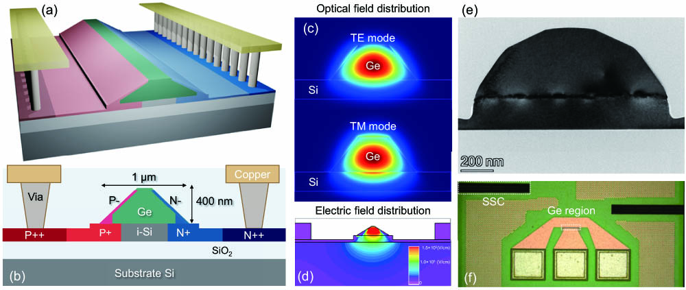
Fig. 1. (a) Three-dimensional (3D) schematic and (b) cross-sectional view of the proposed sidewall doping Ge-Si photodetector. (c), (d) Simulated static optical field and electric field distribution in the Ge region for TE and TM modes. The bias voltage is − 3 V
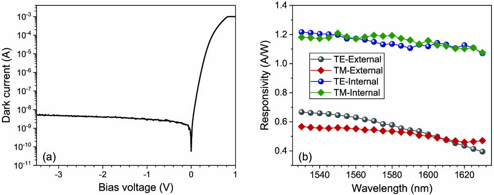
Fig. 2. (a) Current–voltage (I -V ) characteristics of Ge-Si PD in the dark illuminated state. (b) Measured external and calculated internal responsivities of the Ge-Si PD for TE and TM modes in the C + L
Fig. 3. (a) Dark current distribution of PD devices at different reticle sites under − 3 V − 3 V
Fig. 4. Schematic of the experimental setup for measurement of the high-speed eye diagrams. The black and red lines represent optical and electrical connections, respectively. AWG, arbitrary waveform generator; EDFA, erbium doped fiber amplifier; VOA, variable optical attenuator; PC, polarization controller; PD, photodetector; TFLNOI MZM, thin film lithium niobate on insulator Mach–Zehnder modulator.
Fig. 5. Measured 100 Gbaud PAM-4 eye diagrams of TE and TM polarizations under a − 3 V
Fig. 6. Measured 100 Gbaud PAM-4 eye diagrams at 1530, 1550, 1580, and 1610 nm input wavelengths. The time scale is 3 ps/Div. The voltage scale is 6 mV/Div.
Fig. 7. Measured 120, 130, 140, and 150 Gbit/s NRZ eye diagrams under a − 3 V
Fig. 8. Measured 100, 112, 128, and 145 Gbaud PAM-4, and 100, 112, 128, and 136 Gbaud PAM-8 eye diagrams under a − 3 V

Set citation alerts for the article
Please enter your email address
© Copyright 2018-2021 | Chinese Laser Press. All Rights Reserved 沪ICP备15018463号-20