Abstract
Based on the 90 nm silicon photonics commercial foundry, sidewall-doped germanium–silicon photodetectors (PDs) are designed and fabricated. The large designed overlap between the optical field and electric field achieves high responsivity while retaining high-speed performance. Even including the loss due to optical fiber coupling, the PD demonstrates an external responsivity greater than 0.55 A/W for transverse magnetic (TM) polarization and 0.65 A/W for transverse electric (TE) polarization at 1530 nm. A flat responsivity spectrum of is achieved up to 1580 nm for both polarizations. Their internal responsivities can exceed 1 A/W in the optical communication bands. Furthermore, with the aid of a 200 mm wafer-level test and analysis, the overall PDs of 26 reticles have a 3 dB optoelectrical bandwidth and a dark current at a bias voltage. Finally, the eye diagram performances under TE and TM polarizations, various modulation formats, and different input wavelengths are comprehensively investigated. The clear open electrical eye diagrams up to 120, 130, 140, and 150 Gbit/s nonreturn-to-zero are experimentally attained at a photocurrent of 1 mA. To the best of our knowledge, this is the first time that single-lane direct detection of record-high-speed 200, 224, 256, and 290 Gbit/s four-level pulse amplitude modulation (PAM) and 300, 336, 384, and 408 Gbit/s eight-level PAM optical signals has been experimentally achieved.1. INTRODUCTION
Silicon photonics (SiPh) has been identified as a key enabling technology for high-speed data-center interconnects [1], optical input/output (I/O), and copackaged optics [2–4]. It is also a potential solution for future applications in O, E, S, C, and L band coherent telecommunication [5–8]. One of the key building blocks of SiPh is a photodetector (PD) that converts high-speed optical signals to electrical signals [9,10]. An ideal PD should possess high quantum efficiency (QE), low dark current, and the ability to detect ultrahigh-speed optical signals for a single lane [11–14]. Germanium (Ge), possessing large absorption coefficients of up to 1550 nm and even 2000 nm by exploiting tensile-strained bandgap shrinkage, has exhibited excellent photodetection characteristics [15–19]. Various high-speed Ge-Si photodetection structures have been extensively investigated and demonstrated [20–26]. Remarkably, based on the novel biconcave Ge fin shape, a recorded 3 dB cutoff frequency up to 265 GHz has been reported [27], which is an important milestone. Its fabrication processes might be slightly complex. Several hard-masks, lithography, dry etch, and chemical mechanical polishing (CMP) processes are executed to form a lateral Si-Ge-Si p-i-n (PIN) diode and to define the actual width of the Ge region. The QE and dark current should be further improved. The large dark current, which is a direct determinant of the signal-to-noise ratio, will lead to low sensitivity in optical communication systems. So, reducing the dark current is one of the most effective ways to enhance the performance of Ge-Si PD. Additionally, the state-of-the-art Ge-Si high-speed optical detection capability needs to be further boosted [14]. In this scenario, an important goal would be to explore ultrahigh-speed, high-responsivity, and low-dark-current PDs with easy fabrication processes, which is very helpful for realizing low-cost SiPh integrated on-chip optical interconnects.
In European Conference on Optical Communication (ECOC) 2022, we demonstrated a single-lane beyond 400 Gbit/s optical intensity modulation direct detection (IM/DD) system based on a sidewall-doped Ge-Si PD [28]. As an extended version of the work, this paper presents more details about the sidewall-doped Ge-Si PD and gives a comprehensive study of its static and dynamic performances. Based on the commercial 90 nm SiPh platform, we designed and fabricated sidewall-doped Ge-Si PDs, which possess a high electric field () in the Ge region. The internal responsivities of the Ge-Si waveguide PD are larger than 1 A/W at the bands for transverse electric (TE) and transverse magnetic (TM) polarizations, which might benefit from the absorption coefficient improvement by the Franz–Keldysh (FK) effect under a strong electric field. With the aid of an 8-inch wafer-level test and analysis, the overall Ge-Si PDs have a 3 dB optoelectrical (OE) bandwidth and a dark current of less than 10 nA under a bias. Clear open electrical eye diagrams up to 120, 130, 140, and 150 Gbit/s nonreturn-to-zero (NRZ) are experimentally attained. Furthermore, 200, 224, 256, and 290 Gbit/s four-level pulse amplitude modulation (PAM-4) and 300, 336, 384, and 408 Gbit/s eight-level PAM (PAM-8) clear open electrical eye diagrams are also obtained utilizing digital signal processing provided by an oscilloscope at the receiver side.
2. DESIGN AND FABRICATION OF THE Ge-Si PD
Conventional Ge-Si waveguide PDs require heavily doped P- or N-type Ge as well as a metal contact on the Ge area to form the PIN junction. This will lead to a reduced responsivity due to the light absorption of metal contacts. To improve the QE, the double sidewall of the Ge region is lightly doped with P- and N-types to build a lateral PIN junction. Figures 1(a) and 1(b) show the three-dimensional (3D) schematic and cross-sectional view of the proposed sidewall-doped Ge-Si PD with a Si-contacted junction. The designed Ge-Si PDs are fabricated in a commercial 90 nm SiPh platform with simple fabrication processes. The material quality of Ge greatly affects the absorption, carrier transport, and dark current properties. Here, the high-quality Ge film is epitaxially grown on 0.22 μm thick Si through a low-pressure chemical vapor deposition (LPCVD) process with sloped sidewalls, which can be used for P- and N-doping. The tensile strain level of Ge film is in the range of 0.2%–0.22%. An enhanced bandwidth could be achieved with a narrow width of Ge, however, at the expense of growth complexity. Therefore, in this work, the bottom width of the Ge film is designed to be 1 μm with a thickness of approximately 400 nm to achieve a balance among the yield, quality, and bandwidth. The length of the Ge active region is 50 μm to achieve a high QE. The Ge double sidewalls and 220 nm Si waveguide are doped to form the wrapped PIN junction. A gap size of 150 nm is designed for the top P- and N-Ge regions. An approximately 110 nm depth of shallow sidewall doping on Ge is used to minimize the free carrier absorption loss and photogenerated carrier loss in the doped regions. This doping depth unintentionally helps to reduce the intrinsic region of Ge, which is beneficial for decreasing the carrier transit time. The P- and N-doping process is originally used for lateral Ge-on-Si PD, which is conducted on the top of the Ge region. Its doping concentrations and depth are verified satisfactorily by our previously reported high-performance PD structures [12,14,23,24,29]. For the Ge sidewall-doped region, the concentrations of and are designed and optimized to be approximately . For the 220 nm Si slab-doped region, the concentrations of and are approximately . The doping ion implantation energy and dosage are controlled by the SiPh foundry. The left and right bottom corners of the Ge region are also treated with a second doping to reduce the intrinsic Ge, as shown in Fig. 1(b). Figures 1(c) and 1(d) show the simulated static optical field and electric field distribution in the Ge region for TE and TM modes. The maximum intrinsic region of Ge is approximately 450 nm under bias voltage. The overall electric field intensity of the Ge intrinsic region is larger than , which benefits from the well-designed sidewall-doping profiles. The overlaps of the optical field and electric field are very high. It is helpful to enhance the bandwidth and responsivity. The cross-sectional transmission electron microscopy (TEM) image of the Ge-Si PD is shown in Fig. 1(e). The actual width of the bottom Ge is approximately 1.1 μm. The optical micrograph of the proposed Ge-Si PD chip is shown in Fig. 1(f). For the PD responsivity test, the light was coupled via a Si-based suspended spot size conversion (SSC) edge coupler with approximately coupling loss at 1550 nm wavelength.
Sign up for Photonics Research TOC. Get the latest issue of Photonics Research delivered right to you!Sign up now
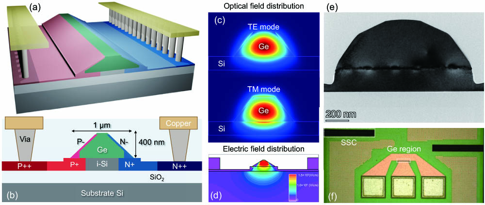
Figure 1.(a) Three-dimensional (3D) schematic and (b) cross-sectional view of the proposed sidewall doping Ge-Si photodetector. (c), (d) Simulated static optical field and electric field distribution in the Ge region for TE and TM modes. The bias voltage is . (e) Transmission electron microscopy (TEM) image of Ge-Si PD. (f) Optical micrograph of the Ge-Si PD. SSC, spot size conversion.
3. EXPERIMENTAL RESULTS
Here, we first study the dark currents versus bias voltages and the dependence of PD responsivities on TE and TM polarizations at the input wavelengths. Then, we analyze the wafer-level distributions of 3 dB bandwidths and dark currents. Then, based on the advanced high-speed large-signal measurement setup and selected Ge-Si PD, the eye diagram performances are comprehensively investigated.
A. Dark Current and Responsivity Measurements
A typical static current–voltage (I-V) characteristic of the selected Ge-Si PD in the dark illuminated state is shown in Fig. 2(a). The chip exhibits dark current as low as 3 and 5 nA at and bias. Here, the external and internal responsivities of the PD are tested. The external responsivity is defined as the photocurrent/fiber input power. The reduction in optical power injection into the PD mainly results from the coupling losses between the single-mode fiber and Si-based SSC. Therefore, for the calculation of internal responsivity, the coupling losses should be excluded. In Fig. 2, the external and internal responsivities of the Ge-Si PD are shown for both TE and TM polarizations (also called TE and TM modes) and marked with “TE-External, TM-External” and “TE-Internal, TM-Internal.” Due to the polarization-dependent loss of SSC, the external responsivity of the TM mode is lower than that of the TE mode. A flat external responsivity spectrum of is achieved up to 1580 nm for both polarizations. The maximum external responsivity of 0.68 A/W is measured at 1530 nm for TE polarization. With further optimization of the SSC coupler, the overall external responsivity spectrum of both modes will be flatter. For longer wavelengths, the responsivity begins to fall off, which is due to the decreased absorption coefficient of Ge [17,30]. However, when the width of Ge is reduced to submicrometer scale, the absorption coefficient can be improved by the FK effect under strong electric field [31]. This will break through the QE of about 60% limitation in the L band. In this work, we also observe the same phenomenon. For TE and TM polarizations, the external responsivities remain at approximately 0.4 A/W up to a wavelength of 1630 nm. These obtained responsivity results are measured at a bias of . The internal responsivity spectra of both modes are also calculated and depicted in Fig. 2(b). It is interesting to note that after the coupling loss power is excluded from the responsivity evaluation, the internal responsivity of TE and TM polarizations can be very high, (approximately equal to the reported value in Ref. [31]) and also approximately equal in the optical communication bands. Their maximum internal responsivities can reach 1.2 A/W.

Figure 2.(a) Current–voltage (I-V) characteristics of Ge-Si PD in the dark illuminated state. (b) Measured external and calculated internal responsivities of the Ge-Si PD for TE and TM modes in the bands.
B. Wafer-Level Distribution of Dark Currents and Bandwidths
The chips are fabricated on an 8-inch Si wafer with 26 reticles. The wafer-level distribution performance is important for mass production. For the wafer-level 3 dB bandwidth test, the light was coupled in via a Si-based C band grating coupler. The measurements of dark currents and 3 dB bandwidths were performed at the wafer level with a Keysight lightwave component analyzer (LCA, N4373D) and a Keithley 2400 source meter. Very low dark currents in the range of 1–10 nA at bias were achieved, as shown in Fig. 3(a). From the TEM image of this Ge-Si PD, as shown in Fig. 1(e), there were many dislocation defects in the Ge-Si buffer, which originated from the foundry process. In conventional vertical PIN structure PDs, the electric field passes vertically through the Ge region, which results in a relatively high electric field intensity at the Ge-Si interface. However, in this sidewall-doped PIN junction, the electric field is approximately horizontal through the Ge region. The electric field intensity in the defect location is relatively small. Additionally, although narrowing the width of Ge to the submicrometer scale (), the tensile lattice strain induced between Ge and the bottom Si due to the thermal expansion mismatch is elastically relaxed by an edge-induced relaxation effect [19,32]. It also benefits a decrease in the dark current. The overall 3 dB OE bandwidths of over 50 GHz are achieved for the 26 reticle sites under a bias condition. The maximum bandwidth is approximately 57 GHz. Here, the 3 dB bandwidth of this device is still mainly limited by the carrier transit time, which might be further optimized by decreasing the bottom width of the Ge region.
Figure 3.(a) Dark current distribution of PD devices at different reticle sites under bias. (b) 3 dB bandwidth distribution of PD devices at different reticle sites under bias.
C. Experimental Setups
A schematic sketch of high-speed NRZ, PAM-4, and PAM-8 eye diagram measurements is illustrated in Fig. 4 [29]. A high-speed RF signal with a word length of is generated by a 256 GSa/s Keysight arbitrary waveform generator (AWG). After amplification by a 67 GHz electrical driver, the RF signal is sent to the thin film lithium niobate on insulator (TFLNOI) C band modulator, which has a 3 dB bandwidth of 60 GHz after advanced packaging, as shown in the left inset of Fig. 4. The electro-optic (EO) response curve is very flat. For the TFLNOI modulator, its 2 dB bandwidth is larger than 67 GHz at the chip level. The available high-bandwidth TFLNOI modulator promises ultrahigh-speed optical signal generation at the transmitter side. A polarization controller (PC) before the modulator is used to change the polarization of light. The fiber-to-fiber insertion losses of the packaged TFLNOI modulator are estimated to be 6.5 dB at 1550 nm wavelength, largely due to the mode mismatch between the optical fiber and SSC. A bias was applied to the selected Ge-Si PD with approximately 55 GHz bandwidth by exploiting an RF probe (cascade infinity probe GSG-150) connected to a 67 GHz bias tee, as shown in the right inset of Fig. 4. For this selected Ge-Si PD, the series resistance and total capacitance are extracted by fitting the scattering parameter data to the small-signal resistor-capacitor (RC) model [12]. The junction capacitance, series resistance, and parasitic capacitance are calculated to be 16.6 fF, , and 11 fF, respectively. The calibration of the high-speed RF trial was implemented to consider the contributions from GSG probes and coaxial cables. Finally, the converted high-speed electrical data were measured with a Keysight sampling oscilloscope without using a transimpedance amplifier (TIA). In our experimental process, to obtain ultrahigh-speed and clear opening eye diagrams with limited 3 dB bandwidths of about 55 GHz, two critical skills are employed. On one hand, the pre-emphasis is carried out in the AWG to compensate for the bandwidth limitation of experimental equipment, the TFLNOI modulator, RF cable, and optical receiver. The compensated 3 dB analog bandwidth of the link is about 73 GHz. On the other hand, the electrical filter provided by sampling oscilloscope is utilized to reduce the high-speed signal noise.
Figure 4.Schematic of the experimental setup for measurement of the high-speed eye diagrams. The black and red lines represent optical and electrical connections, respectively. AWG, arbitrary waveform generator; EDFA, erbium doped fiber amplifier; VOA, variable optical attenuator; PC, polarization controller; PD, photodetector; TFLNOI MZM, thin film lithium niobate on insulator Mach–Zehnder modulator.
D. Eye Diagram Performances
The feasibility of this Ge-Si PD is further checked by measuring the eye diagram large-signal acquisitions with two polarization states, different input optical wavelengths, different operation speeds, and various modulation formats. As shown in Fig. 2, the internal responsivities of the TE and TM modes are nearly equal in all communication bands. A high-speed and high-responsivity polarization-insensitive PD, which allows a standard single-mode fiber interconnection to the link and reduces receiver complexity, is highly desirable for data-center, 5G or future 6G wireless networks. There have been existing modulators that feature polarization-insensitive operation in the communication bands [33,34]. Here, as shown in Fig. 5, based on this Ge-Si PD, the 100 Gbaud PAM-4 (200 Gbit/s) modulation clear opening of eye diagrams of TE and TM polarizations under a bias at 1550 nm wavelength is experimentally obtained. For TE mode, the time-averaged output photocurrent value is about 1.31 mA. However, for TM mode, its output photocurrent is 1.25 mA even under the same input optical power. There still exists a little difference in dynamic characteristics. These results exhibit the great potential for applications in polarization-insensitive high-speed signal reception.
Figure 5.Measured 100 Gbaud PAM-4 eye diagrams of TE and TM polarizations under a bias voltage at 1550 nm input wavelength. The time scale is 3 ps/Div. The voltage scale is 6 mV/Div.
The ever-increasing requirement for enhanced data transmission capacity has inspired the investigation of ultrawideband optical communication, which includes C and L bands. Since the communication capacity of the C band with high-speed coherent technologies for long-haul transmission approaches the Shannon limit, extending the frequency bands (from the C band to the or bands) will be the optimal path to further enhance the capacity of a single-mode fiber. In the 2016 Optical Fiber Communication Conference Postdeadline Paper (OFC-PDP), the O, E, S, C, and L band monolithic silicon photonic integrated coherent modulator and receiver were presented. However, the details and high-speed performances of the PD were not described. Here, we study the IM/DD characteristic in the bands based on our designed PD. As shown in Fig. 6, the 100 Gbaud PAM-4 (200 Gbit/s) modulation clear opening eye diagrams at 1530, 1550, 1580, and 1610 nm wavelengths are obtained. The bias voltage is with approximately 1 mA DC. It is obvious that the quality of the eye diagram deteriorates slightly at 1610 nm, which might be due to the influence of the TFLNOI modulator and responsivity reduction of Ge-Si PD. In this experimental process, the modulator working bias point is synchronously tuned with the change in input optical wavelength. However, the optical power injected into the Ge-Si PD is fixed at different wavelengths. At longer wavelengths (L band), the mismatch of the effective index of the electrical signal and the group index of the optical signal would lead to high-speed eye diagram degradation of the C band TFLNOI modulator.
Figure 6.Measured 100 Gbaud PAM-4 eye diagrams at 1530, 1550, 1580, and 1610 nm input wavelengths. The time scale is 3 ps/Div. The voltage scale is 6 mV/Div.
As shown in Fig. 7, clear open electrical eye diagrams up to 120, 130, 140, and 150 Gbit/s NRZ are also attained for the first time by using the proposed Ge-Si PD at a photocurrent of 1 mA. The ultrahigh-speed optical signal reception capability primarily results from the high bandwidth (), high responsivity (), and low dark current () of this device.
Figure 7.Measured 120, 130, 140, and 150 Gbit/s NRZ eye diagrams under a bias voltage. The time scale is 3 ps/Div.
The PAM-N modulation format is an efficient way to obtain a higher bit rate with a limited 3 dB bandwidth. To further increase the high-speed signal reception capability, PAM-4 and PAM-8 modulations are also investigated. Clear open eye diagrams up to 100, 112, 128, and 145 Gbaud PAM-4 and 100, 112, 128, and 136 Gbaud PAM-8 are obtained with the help of pre-emphasis at the transmitter side and electrical filter at the receiver side, as shown in Fig. 8. To the best of our knowledge, we report for the first time a SiPh PD operating at per lane in an IM/DD system. We believe that the proposed sidewall doping PD devices possess great potential to achieve low-cost data reception per lane for future 800G/1.6T data centers. Additionally, the flat and high responsivity in a broad optical range can simultaneously support O, S, C, and L band coherent transmission systems. Overall, the sidewall-doped Ge-Si PD achieves a good trade-off among bandwidth, dark current, responsivity, and fabrication process complexity. In the near future, by utilizing the advanced co-design of electronics and photonics components and flip-chip bonding technology, it is possible to realize a high-speed 3D-integrated SiPh receiver with sub-pJ/bit power consumption [35–39].
Figure 8.Measured 100, 112, 128, and 145 Gbaud PAM-4, and 100, 112, 128, and 136 Gbaud PAM-8 eye diagrams under a bias voltage with approximately 0.8 mA DC. The time scale is 3 ps/Div.
4. CONCLUSIONS
Based on the available 90 nm SiPh foundry, we design and fabricate sidewall-doped Ge-Si PDs. The internal responsivities of TE and TM polarizations are larger than 1 A/W in the bands. With the aid of wafer-level testing and analysis, the overall PDs have bandwidths larger than 50 GHz and dark currents less than 10 nA under a bias. Utilizing this PD, 200 Gbit/s PAM-4 eye diagrams are obtained for both TE and TM polarizations at an input wavelength of 1550 nm. They can also support the speed of 200 Gbit/s signal reception at 1530, 1550, 1580, and 1610 nm wavelengths. Additionally, clear open electrical eye diagrams up to 120, 130, 140, and 150 Gbit/s NRZ are experimentally attained. The 200, 224, 256, and 290 Gbit/s PAM-4 and 300, 336, 384, and 408 Gbit/s PAM-8 clear open electrical eye diagrams are also obtained by utilizing digital signal processing provided by an oscilloscope at the receiver side. To the best of our knowledge, this is the first reported Ge-Si PD operating at for a single lane in an IM/DD system, which is very helpful for realizing low-cost integrated SiPh co-packaged optics (CPO) in the future. It can also support ultrawide band () coherent transmission systems.
References
[1] Y. Zhao, L. Chen, R. Aroca, N. Zhu, D. Ton, D. Inglis, C. R. Doerr. Silicon photonic based stacked die assembly toward 4 × 200-Gbit/s short-reach transmission. J. Lightwave Technol., 40, 1369-1374(2022).
[2] S. Fathololoumi, D. Hui, S. Jadhav, J. Chen, K. Nguyen, M. N. Sakib, Z. Li, H. Mahalingam, S. Amiralizadeh, N. N. Tang, H. Potluri, M. Montazeri, H. Frish, R. A. Defrees, C. Seibert, A. Krichevsky, J. K. Doylend, J. Heck, R. Venables, A. Dahal, A. Awujoola, A. Vardapetyan, G. Kaur, M. Cen, V. Kulkarni, S. S. Islam, R. L. Spreitzer, S. Garag, A. C. Alduino, R. K. Chiou, L. Kamyab, S. Gupta, B. Xie, R. S. Appleton, S. Hollingsworth, S. McCargar, Y. Akulova, K. M. Brown, R. Jones, D. Zhu, T. Liljeberg, L. Liao. 1.6 Tbps silicon photonics integrated circuit and 800 Gbps photonic engine for switch co-packaging demonstration. J. Lightwave Technol., 39, 1155-1161(2021).
[3] K. Hosseini, E. Kok, S. Y. Shumarayev, C.-P. Chiu, A. Sarkar, A. Toda, Y. Ke, A. Chan, D. Jeong, M. Zhang, S. Raman, T. Tran, K. A. Singh, P. Bhargava, C. Zhang, H. Lu, R. Mahajan, X. Li, N. Deshpande, C. O'Keeffe, T. T. Hoang, U. Krishnamoorthy, C. Sun, R. Meade, V. Stojanovic, M. Wade. 8 Tbps co-packaged FPGA and silicon photonics optical IO. Optical Fiber Communication Conference, Th4A.2(2021).
[4] L. Liao, S. Fathololoumi, D. Hui. High density silicon photonic integrated circuits and photonic engine for optical co-packaged Ethernet switch. European Conference on Optical Communication, Tu2C.1(2020).
[5] C. Doerr, L. Chen, T. Nielsen, R. Aroca, L. Chen, M. Banaee, S. Azemati, G. McBrien, S. Y. Park, J. Geyer, B. Guan. O, E, S, C, and L band silicon photonics coherent modulator/receiver. Optical Fiber Communication Conference, Th5C.4(2016).
[6] P. M. Seiler, K. Voigt, A. Peczek, G. Georgieva, S. Lischke, A. Malignaggi, L. Zimmermann. Multiband silicon photonic ePIC coherent receiver for 64 GBd QPSK. J. Lightwave Technol., 40, 3331-3337(2022).
[7] R. Emmerich, M. Ribeiro Sena, R. Elschner, C. Schmidt-Langhorst, I. Sackey, C. Schubert, R. Freund. Enabling S-C-L-band systems with standard C-band modulator and coherent receiver using coherent system identification and nonlinear predistortion. J. Lightwave Technol., 40, 1360-1368(2022).
[8] G. Rademacher, R. S. Luís, B. J. Puttnam, R. Ryf, S. van der Heide, T. A. Eriksson, N. K. Fontaine, H. Chen, R. Essiambre, Y. Awaji, H. Furukawa, N. Wada. 172 Tb/s C+L band transmission over 2040 km strongly coupled 3-Core fiber. Optical Fiber Communication Conference, Th4B.5(2020).
[9] J. Michel, J. Liu, L. C. Kimerling. High-performance Ge-on-Si photodetectors. Nat. Photonics, 4, 527-534(2010).
[10] D. Benedikovic, L. Virot, G. Aubin, J. Hartmann, F. Amar, X. L. Roux, C. Alonso-Ramos, E. Cassan, D. Marris-Morini, J. Fédéli, F. Boeuf, B. Szelag, L. Vivien. Silicon-germanium receivers for short-wave-infrared optoelectronics and communications. Nanophotonics, 10, 1059-1079(2020).
[11] X. Hu, D. Wu, D. Chen, L. Wang, X. Xiao, S. Yu. 180 Gbit/s Si3N4-waveguide coupled germanium photodetector with improved quantum efficiency. Opt. Lett., 46, 6019-6022(2021).
[12] X. Hu, D. Wu, H. Zhang, W. Li, D. Chen, L. Wang, X. Xiao, S. Yu. High-speed and high-power germanium photodetector with a lateral silicon nitride waveguide. Photon. Res., 9, 749-756(2021).
[13] H. Chen, M. Galili, P. Verheyen, P. De Heyn, G. Lepage, J. De Coster, S. Balakrishnan, P. Absil, L. Oxenlowe, J. Van Campenhout, G. Roelken. 100-Gbps RZ data reception in 67-GHz Si-contacted germanium waveguide p-i-n photodetectors. J. Lightwave Technol., 35, 722-726(2017).
[14] D. Chen, H. Zhang, M. Liu, X. Hu, Y. Zhang, D. Wu, P. Zhou, S. Chang, L. Wang, X. Xiao. 67 GHz Light-trapping-structure germanium photodetector supporting 240 Gb/s PAM-4 transmission. Photon. Res., 10, 2165-2171(2022).
[15] Y. Ishikawa, K. Wada, D. D. Cannan, J. Liu, H.-C. Luan, L. C. Kimerling. Strain-induced band gap shrinkage in Ge grown on Si substrate. Appl. Phys. Lett., 82, 2044-2046(2003).
[16] D. D. Cannon, J. Liu, Y. Ishikawa, K. Wada, D. T. Danielson, S. Jongthammanurak, J. Michel, L. C. Kimerling. Tensile strained epitaxial Ge films on Si (100) substrates with potential application in L-band telecommunications. Appl. Phys. Lett., 84, 906-908(2004).
[17] J. Liu, D. D. Cannon, K. Wada, Y. Ishikawa, S. Jongthammanurak, D. T. Danielson, J. Michel, L. C. Kimerling. Tensile strained Ge p-i-n photodetectors on Si platform for C and L band telecommunications. Appl. Phys. Lett., 87, 011110(2005).
[18] J. Liu, J. Michel, W. Giziewicz, D. Pan, K. Wada, D. Cannon, L. C. Kimerling, J. Chen, F. O. Ilday, F. X. Kartner, J. Yasaitis. High performance, tensile strained Ge p-i-n photodetectors on a Si platform. Appl. Phys. Lett., 87, 103501(2005).
[19] R. Anthony, D. E. Hagan, D. Genuth-Okon, L. M. Maestro, I. F. Crowe, M. P. Halsall, A. P. Knights. Extended wavelength responsivity of a germanium photodetector integrated with a silicon waveguide exploiting the indirect transition. IEEE J. Sel. Top. Quantum Electron., 26, 3800107(2020).
[20] C. T. DeRose, D. C. Trotter, W. A. Zortman, A. L. Starbuck, M. Fisher, M. R. Watts, P. S. Davids. Ultra compact 45 GHz CMOS compatible germanium waveguide photodiode with low dark current. Opt. Express, 19, 24897-24904(2011).
[21] L. Vivien, A. Polzer, D. Marris-Morini, J. Osmond, J. M. Hartmann, P. Crozat, E. Cassan, C. Kopp, H. Zimmermann, J. M. Fédéli. Zero-bias 40 Gbit/s germanium waveguide photodetector on silicon. Opt. Express, 20, 1096-1101(2012).
[22] S. Lischke, D. Knoll, C. Mai, L. Zimmermann, A. Peczek, M. Kroh, A. Trusch, E. Krune, K. Voigt, A. Mai. High bandwidth, high responsivity waveguide-coupled germanium pin photodiode. Opt. Express, 23, 27213-27220(2015).
[23] X. Hu, D. Wu, H. Zhang, W. Li, D. Chen, L. Wang, X. Xiao, S. Yu. High-speed lateral PIN germanium photodetector with 4-directional light input. Opt. Express, 28, 38343-38354(2020).
[24] D. Y. Wu, X. Hu, W. Z. Li, D. G. Chen, L. Wang, X. Xiao. 62 GHz germanium photodetector with inductive gain peaking electrode for photonic receiving beyond 100 Gbaud. J. Semicond., 42, 020502(2021).
[25] D. Benedikovic, L. Virot, G. Aubin, F. Amar, B. Szelag, B. Karakus, J. M. Hartmann, C. Alonso-Ramos, X. L. Roux, P. Crozat, E. Cassan, D. Marris-Morini, C. Baudot, F. Boeuf, J. M. Fédéli, C. Kopp, L. Vivien. 25 Gbps low-voltage hetero-structured silicon-germanium waveguide pin photodetectors for monolithic on-chip nanophotonic architectures. Photon. Res., 7, 437-444(2019).
[26] D. Benedikovic, L. Virot, G. Aubin, J. M. Hartmann, F. Amar, B. Szelag, X. L. Roux, C. Alonso-Ramos, P. Crozat, É. Cassan, D. Marris-Morini, C. Baudot, F. Boeuf, J. M. Fédéli, C. Kopp, L. Vivien. Comprehensive study on chip-integrated germanium PIN photodetectors for energy-efficient silicon interconnects. IEEE J. Quantum Electron., 56, 8400409(2020).
[27] S. Lischke, A. Peczek, J. S. Morgan, K. Sun, D. Steckler, Y. Yamamoto, F. Korndörfer, C. Mai, S. Marschmeyer, M. Fraschke, A. Krüger. Ultra-fast germanium photodiode with 3 dB bandwidth of 265 GHz. Nat. Photonics, 15, 925-931(2021).
[28] X. Hu, D. Wu, Y. Liu, M. Liu, J. Liu, H. Zhang, Y. Zhang, D. Chen, L. Wang, X. Xiao, S. Yu. Single lane beyond 400 Gbit/s optical direct detection based on a sidewall-doped Ge-Si photodetector. European Conference on Optical Communication, Th2E.5(2022).
[29] X. Hu, H. Zhang, D. Wu, D. Chen, L. Wang, X. Xiao, S. Yu. High-performance germanium avalanche photodetector for 100 Gbit/s photonics receivers. Opt. Lett., 46, 3837-3840(2021).
[30] N. N. Feng, P. Dong, D. Zheng, S. Liao, H. Liang, R. Shafiiha, D. Feng, G. Li, J. E. Cunningham, A. V. Krishnamoorthy, M. Asghari. Vertical pin germanium photodetector with high external responsivity integrated with large core Si waveguides. Opt. Express, 18, 96-101(2009).
[31] S. A. Srinivasan, M. Pantouvaki, S. Gupta, H. T. Chen, P. Verheyen, G. Lepage, G. Roelkens, K. Saraswat, D. Van Thourhout, P. Absil, J. Van Campenhout. 56 Gb/s germanium waveguide electro-absorption modulator. J. Lightwave Technol., 34, 419-424(2016).
[32] S. Sonoi, R. Katamawari, M. Shimokawa, K. Inaba, J. A. Piedra-Lorenzana, T. Hizawa, J. Fujikata, Y. Ishikawa. Direct bandgap control by narrowing the germanium strip structure on silicon for C+L band photonic devices. IEEE J. Quantum Electron., 58, 8400209(2022).
[33] X. Hu, J. Wang. Design of graphene-based polarization-insensitive optical modulator. Nanophotonics, 7, 651-658(2018).
[34] Y. Pan, M. He, M. Xu, Z. Lin, Y. Lin, W. Ke, J. Liu, Z. Lin, Y. Zhu, S. Gao, H. Li, X. Liu, C. Liu, S. Liu, X. Cai. Compact substrate-removed thin-film lithium niobate electro-optic modulator featuring polarization-insensitive operation. Opt. Lett., 47, 1818-1821(2022).
[35] K. Li, S. Liu, X. Ruan, D. J. Thomson, Y. Hong, F. Yang, L. Zhang, C. Lacava, F. Meng, W. Zhang, P. Petropoulos. Co-design of a differential transimpedance amplifier and balanced photodetector for a sub-pJ/bit silicon photonics receiver. Opt. Express, 28, 14038-14054(2020).
[36] S. Saeedi, S. Menezo, G. Pares, A. Emami. A 25 Gb/s 3D-integrated CMOS/silicon-photonic receiver for low-power high-sensitivity optical communication. J. Lightwave Technol., 34, 2924-2933(2016).
[37] D. Wu, D. Wang, D. Chen, J. Yan, Z. Dang, J. Feng, S. Chen, P. Feng, H. Zhang, Y. Fu, L. Wang, X. Hu, X. Xiao, S. Yu. Experimental demonstration of a 160 Gbit/s 3D-integrated silicon photonics receiver with 1.2-pJ/bit power consumption. Opt. Express, 31, 4129-4139(2023).
[38] G. Dziallas, A. Fatemi, A. Malignaggi, G. Kahmen. A 97-GHz 66-dBΩ SiGe BiCMOS low-noise transimpedance amplifier for optical receivers. IEEE Microw. Wireless Compon. Lett., 31, 1295-1298(2021).
[39] I. G. López, A. Awny, P. Rito, M. Ko, A. C. Ulusoy, D. Kissinger. 100 Gb/s differential linear TIAs with less than 10 pA/Hz in 130-nm SiGe:C BiCMOS. IEEE J. Solid-State Circuits, 53, 458-469(2018).


