• Chinese Physics B
  • Vol. 29, Issue 9, (2020)
Xiaozhang Chen1, Lehua Gu2, Lan Liu1, Huawei Chen1, Jingyu Li1, Chunsen Liu3、†, and Peng Zhou1
Author Affiliations
  • 1The State Key Laboratory of ASIC and System, Department of Microelectronics, Fudan University, Shanghai 200433, China
  • 2Department of Physics, State Key Laboratory of Surface Physics, Key Laboratory of Micro and Nano Photonic Structures (Ministry of Education), and Institute for Nanoelectronic Devices and Quantum Computing, Fudan University, Shanghai 00433, China
  • 3School of Computer Science, Fudan University, Shanghai 2004, China
  • show less
    DOI: 10.1088/1674-1056/aba9cf Cite this Article
    Xiaozhang Chen, Lehua Gu, Lan Liu, Huawei Chen, Jingyu Li, Chunsen Liu, Peng Zhou. Temperature-switching logic in MoS2 single transistors[J]. Chinese Physics B, 2020, 29(9): Copy Citation Text show less
    The thickness of the top and bottom h-BN layers in the MoS2 logic transistor confirmed by the atomic force microscope. The top h-BN is 6 nm and bottom h-BN is 8 nm.
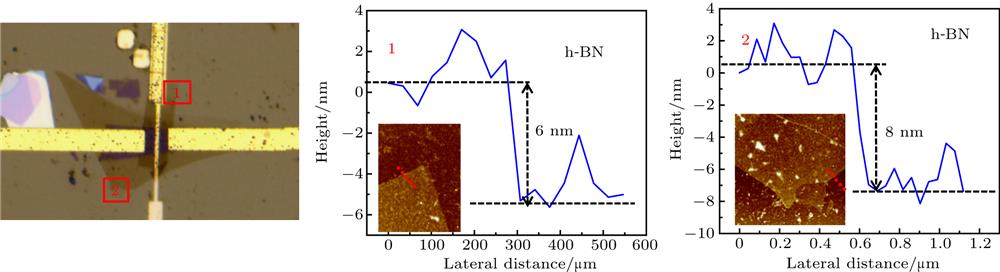
    Fig. 1. The thickness of the top and bottom h-BN layers in the MoS2 logic transistor confirmed by the atomic force microscope. The top h-BN is 6 nm and bottom h-BN is 8 nm.
    Device structure and characterization of MoS2 logic transistor. (a) Three-dimensional sectional view of MoS2 logic transistor. MoS2 serves as channel material; h-BN serves as dielectric material; top and bottom gates are used to input logic signal (voltage); drain and source are used to collect output signal (current). (b) Raman spectra of MoS2 logic transistor, obtained by laser with 532 nm wavelength and 50 μW energy. The overlapped region shows characteristic peaks of the two materials (MoS2 and h-BN). (c) Temperature switchable logic output of MoS2 logic transistor. Continuous ± 2 V is provided as input signal through top and bottom gates; channel current is collected as an output signal through drain and source; the drain voltage is 500 mV. The output characteristic of this device can be transformed into voltage by load resistance which is shown in Figs. A3–A5.
    Fig. 1. Device structure and characterization of MoS2 logic transistor. (a) Three-dimensional sectional view of MoS2 logic transistor. MoS2 serves as channel material; h-BN serves as dielectric material; top and bottom gates are used to input logic signal (voltage); drain and source are used to collect output signal (current). (b) Raman spectra of MoS2 logic transistor, obtained by laser with 532 nm wavelength and 50 μW energy. The overlapped region shows characteristic peaks of the two materials (MoS2 and h-BN). (c) Temperature switchable logic output of MoS2 logic transistor. Continuous ± 2 V is provided as input signal through top and bottom gates; channel current is collected as an output signal through drain and source; the drain voltage is 500 mV. The output characteristic of this device can be transformed into voltage by load resistance which is shown in Figs. A3A5.
    The false-colored SEM image of MoS2 logic transistor. The blue represents h-BN; red represents the MoS2; yellow represents electrodes.
    Fig. 2. The false-colored SEM image of MoS2 logic transistor. The blue represents h-BN; red represents the MoS2; yellow represents electrodes.
    Temperature dependence of MoS2 logic transistor. (a) The current density distribution diagram at different temperatures. (b) The current distribution histogram of four states at different temperatures. The asymmetric performance of IN-01 and IN-10 is caused by different thickness of h-BN, which leads to the abnormal logic function (neither ‘OR’ nor ‘AND’) at 50 K, 100 K, and 150 K. Both (a) and (b) have the same input voltage (VTG, VBG = ±2 V), VD = 500 mV, and color bar.
    Fig. 2. Temperature dependence of MoS2 logic transistor. (a) The current density distribution diagram at different temperatures. (b) The current distribution histogram of four states at different temperatures. The asymmetric performance of IN-01 and IN-10 is caused by different thickness of h-BN, which leads to the abnormal logic function (neither ‘OR’ nor ‘AND’) at 50 K, 100 K, and 150 K. Both (a) and (b) have the same input voltage (VTG, VBG = ±2 V), VD = 500 mV, and color bar.
    The temperature dependence of Fermi–Dirac distribution function of MoS2 logic transistor. (a) Schematic diagrams of temperature influence on the Fermi–Dirac distribution function. The schematic diagram shows the change process of Fermi–Dirac distribution function with temperature intuitively. (b) Photoluminescence spectrum of MoS2 logic transistor at different temperatures (10–250 K). The excitation wavelength is 532 nm; power is 40 μW; integration time is 10 s. (c) The decrease tendency of direct and indirect band gaps of MoS2 logic transistor with increasing temperature.
    Fig. 3. The temperature dependence of Fermi–Dirac distribution function of MoS2 logic transistor. (a) Schematic diagrams of temperature influence on the Fermi–Dirac distribution function. The schematic diagram shows the change process of Fermi–Dirac distribution function with temperature intuitively. (b) Photoluminescence spectrum of MoS2 logic transistor at different temperatures (10–250 K). The excitation wavelength is 532 nm; power is 40 μW; integration time is 10 s. (c) The decrease tendency of direct and indirect band gaps of MoS2 logic transistor with increasing temperature.
    The circuit of MoS2 logic transistor that outputs the current signal. IN 1 and IN 2 separately represent the input signal from the top gate and bottom gate. The input voltage is generated by Keithley 4200 A semiconductor parameter analyzer. And output current is measured by the same instrument.
    Fig. 3. The circuit of MoS2 logic transistor that outputs the current signal. IN 1 and IN 2 separately represent the input signal from the top gate and bottom gate. The input voltage is generated by Keithley 4200 A semiconductor parameter analyzer. And output current is measured by the same instrument.
    The circuit of MoS2 logic transistor that outputs voltage signal. To transfer output current into voltage, a resistor (220 kΩ) is induced into the circuit. An oscilloscope is used to measure the partial voltage of the resistor.
    Fig. 4. The circuit of MoS2 logic transistor that outputs voltage signal. To transfer output current into voltage, a resistor (220 kΩ) is induced into the circuit. An oscilloscope is used to measure the partial voltage of the resistor.
    Temperature dependence of mobility, threshold voltage, and saturation current. (a) and (b) The transfer characteristics of the top gate and bottom gate in MoS2 logic transistor. Panels (a) and (b) use the same graphic symbol. (c) The extracted mobility and subthreshold voltage at various temperatures. (d) The saturation current extracted from (a) and (b) at 2 V under various temperatures.
    Fig. 4. Temperature dependence of mobility, threshold voltage, and saturation current. (a) and (b) The transfer characteristics of the top gate and bottom gate in MoS2 logic transistor. Panels (a) and (b) use the same graphic symbol. (c) The extracted mobility and subthreshold voltage at various temperatures. (d) The saturation current extracted from (a) and (b) at 2 V under various temperatures.
    Diagram of the voltage output of MoS2 logic transistor. The resistance is 220 kΩ and the measuring instrument is oscilloscope (internal resistance = 1 MΩ). However, the oscilloscope internal resistance is not large enough for two-dimensional material devices, which makes the branch current of the oscilloscope very big. Therefore the voltage output of the device has a low on–off ratio after transformation.
    Fig. 5. Diagram of the voltage output of MoS2 logic transistor. The resistance is 220 kΩ and the measuring instrument is oscilloscope (internal resistance = 1 MΩ). However, the oscilloscope internal resistance is not large enough for two-dimensional material devices, which makes the branch current of the oscilloscope very big. Therefore the voltage output of the device has a low on–off ratio after transformation.
    The dual-sweep transfer curves of MoS2 logic transistor. The zero hysteresis indicates that the interface charge trapping is negligible; VD = 500 mV, T = 250 K.
    Fig. 6. The dual-sweep transfer curves of MoS2 logic transistor. The zero hysteresis indicates that the interface charge trapping is negligible; VD = 500 mV, T = 250 K.
    Xiaozhang Chen, Lehua Gu, Lan Liu, Huawei Chen, Jingyu Li, Chunsen Liu, Peng Zhou. Temperature-switching logic in MoS2 single transistors[J]. Chinese Physics B, 2020, 29(9):
    Download Citation