
Sheng-Yu RAO, Chun-Qi SHI, Run-Xi ZHANG. A CMOS millimetre wave down-conversion mixer for 76-81 GHz automotive radars [J]. Journal of Infrared and Millimeter Waves, 2020, 39(4): 441
- Journal of Infrared and Millimeter Waves
- Vol. 39, Issue 4, 441 (2020)
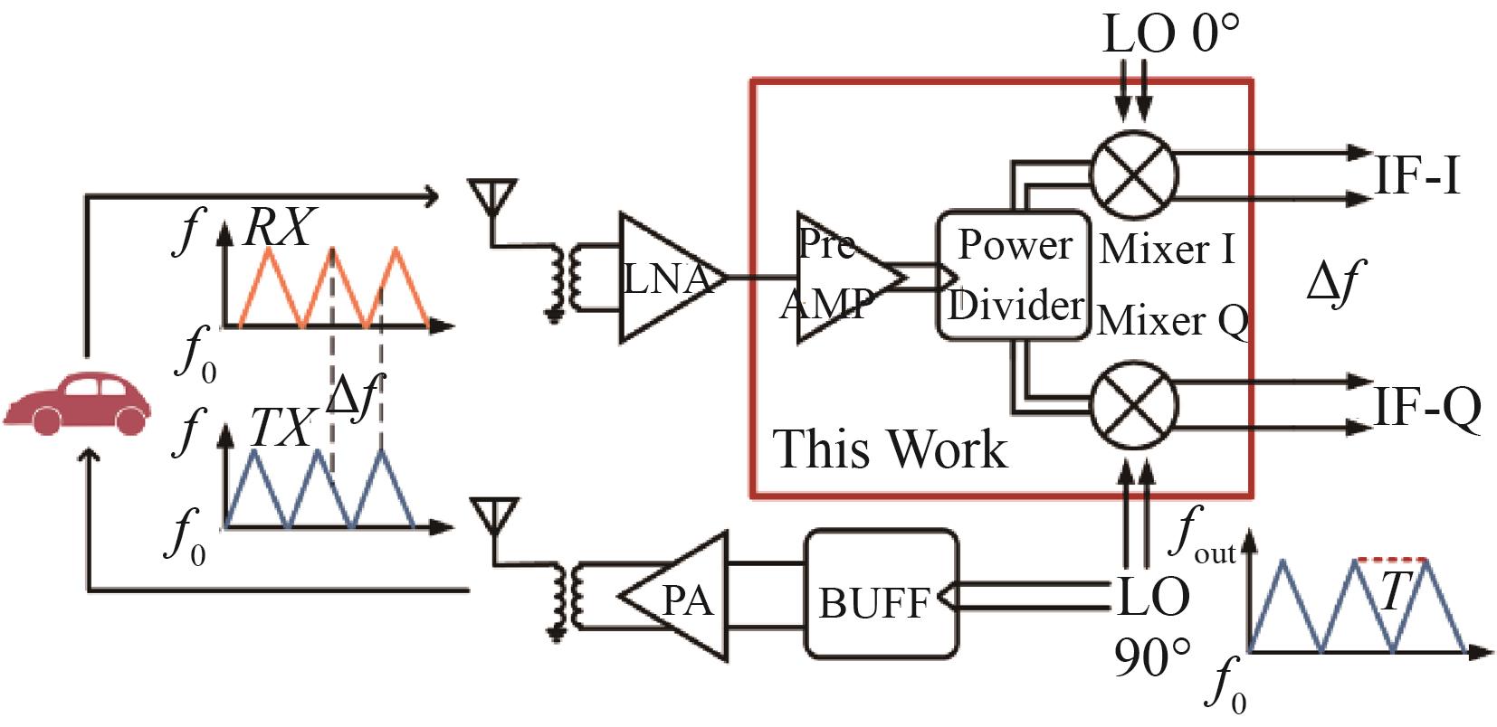
Fig. 1. Block diagram of the proposed 76~81 GHz quadrature transceiver
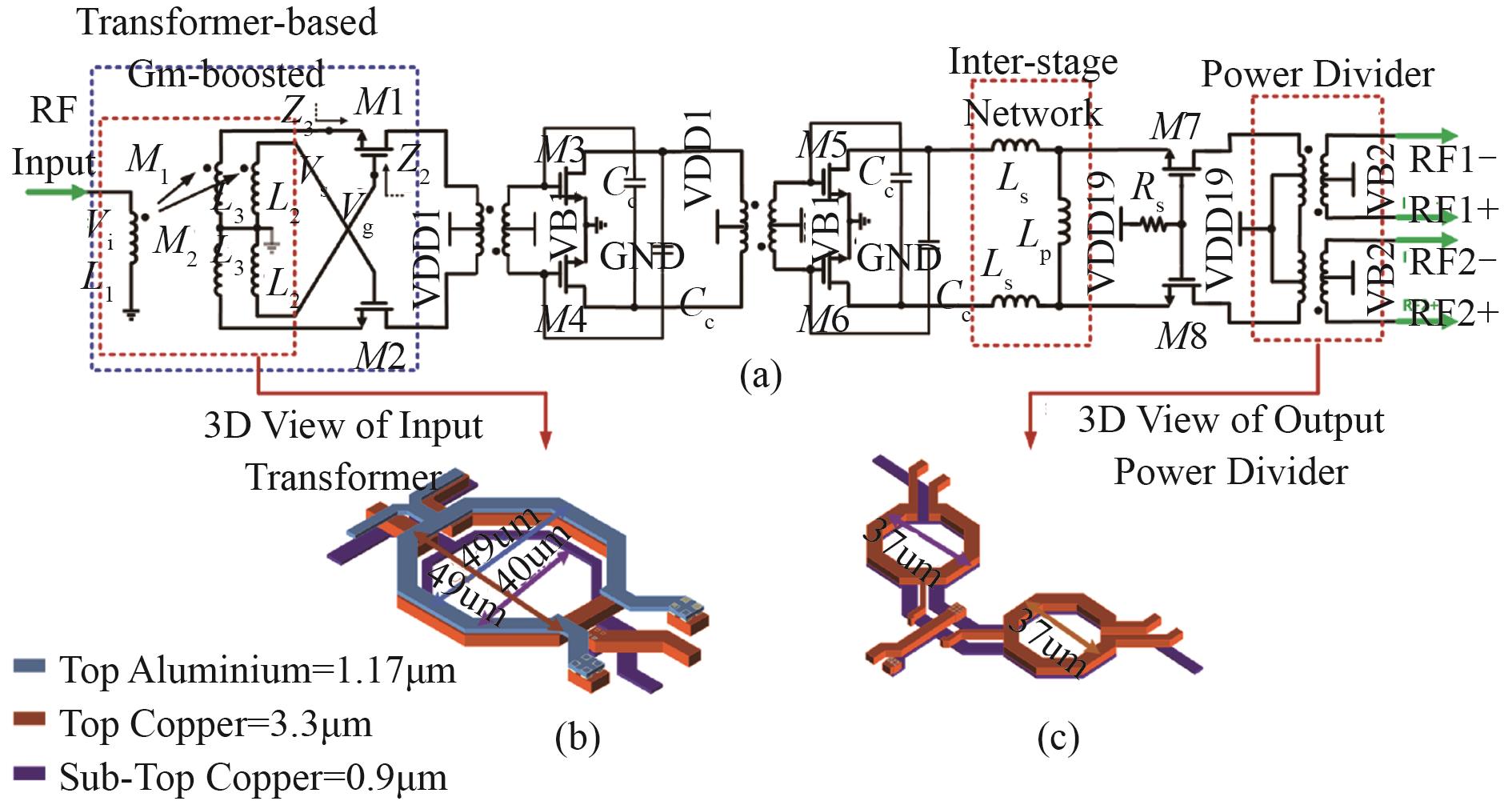
Fig. 2. (a) Schematic of the pre-amplifier with a transformer-based gm-boosted network and output power divider, (b) 3D view of the input transformer, and (c) 3D view of the output power divider.
Fig. 3. Simulated results of the gm-boosted single-stage CS amplifier
Fig. 4. (a) Inter-stage serial inductance network, (b) Inter-stage serial-parallel resonating network, and (c) The proposed LC resonating network
Fig. 5. Simulated results of the inter-stage parasitic capacitance elimination network
Fig. 6. (a) The schematic of proposed active mixer, (b) equivalent model of active mixer inter-stage impedance, and (c) noise model of active mixer and the schematic of dynamic current-bleeding.
Fig. 7. Simulated conversion gain of the active mixer using various architectures
Fig. 8. Chip photograph
Fig. 9. Measured S11 of the down-conversion mixer
Fig. 10. Measured CG of the down-conversion mixer
Fig. 11. Measured input P1dB of the down-conversion mixer
Fig. 12. Measured noise figure of the down-conversion mixer
|
Table 1. 本文正交下混频器测试性能总结及与已报道混频器的性能对比(25 ℃)

Set citation alerts for the article
Please enter your email address
© Copyright 2018-2021 | Chinese Laser Press. All Rights Reserved 沪ICP备15018463号-20