• Photonics Research
  • Vol. 11, Issue 8, 1465 (2023)
DaeHwan Ahn1、†, Sunghan Jeon1、2、†, Hoyoung Suh1, Seungwan Woo1, Rafael Jumar Chu1, Daehwan Jung1, Won Jun Choi1, Donghee Park1, Jin-Dong Song1, Woo-Young Choi2, and Jae-Hoon Han1、*
Author Affiliations
  • 1Center for Opto-Electronic Materials and Devices, Korea Institute of Science and Technology (KIST), Seoul 02792, Republic of Korea
  • 2Department of Electrical and Electronic Engineering, Yonsei University, Seoul 03722, Republic of Korea
  • show less
    DOI: 10.1364/PRJ.491498 Cite this Article Set citation alerts
    DaeHwan Ahn, Sunghan Jeon, Hoyoung Suh, Seungwan Woo, Rafael Jumar Chu, Daehwan Jung, Won Jun Choi, Donghee Park, Jin-Dong Song, Woo-Young Choi, Jae-Hoon Han. High-responsivity InAs quantum well photo-FET integrated on Si substrates for extended-range short-wave infrared photodetector applications[J]. Photonics Research, 2023, 11(8): 1465 Copy Citation Text show less
    (a) Fabrication flow of InAs QW photo-FETs integrated on SiO2 interlayer dielectric (ILD)/Si substrates using direct wafer bonding techniques. (b) Optical microscope (OM) and (c) TEM images of a transferred III-V layer on Si substrates using Au/Au metal bonding.
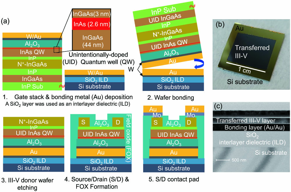
    Fig. 1. (a) Fabrication flow of InAs QW photo-FETs integrated on SiO2 interlayer dielectric (ILD)/Si substrates using direct wafer bonding techniques. (b) Optical microscope (OM) and (c) TEM images of a transferred III-V layer on Si substrates using Au/Au metal bonding.
    (a) Schematic image of an InAs QW photo-FET. (b) High-angle annular dark-field scanning TEM (HAADF-STEM) image of an InAs QW photo-FET, confirming successful selective etching of N+-InGaAs source/drain (S/D) regions. High-resolution TEM image shows (c) an InAs QW channel. (d) PL spectrum and (e) energy band diagram of InAs QW structures. The band edge values of the conduction band and valence band for compressively strained InAs (s-InAs) were used to calculate the sub-band energies for an electron (E1) and a heavy hole (HH1). (f) Calculated wavelength peak of the InAs QW as a function of the InAs thickness.
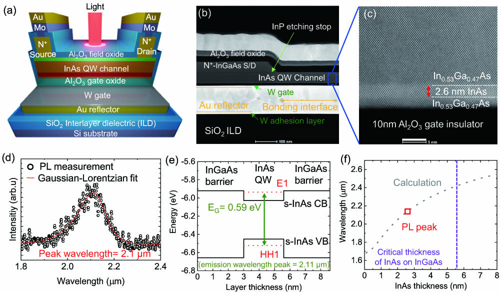
    Fig. 2. (a) Schematic image of an InAs QW photo-FET. (b) High-angle annular dark-field scanning TEM (HAADF-STEM) image of an InAs QW photo-FET, confirming successful selective etching of N+-InGaAs source/drain (S/D) regions. High-resolution TEM image shows (c) an InAs QW channel. (d) PL spectrum and (e) energy band diagram of InAs QW structures. The band edge values of the conduction band and valence band for compressively strained InAs (s-InAs) were used to calculate the sub-band energies for an electron (E1) and a heavy hole (HH1). (f) Calculated wavelength peak of the InAs QW as a function of the InAs thickness.
    (a) Measurement configuration based on the confocal microscopy. (b) ID-VG curves of InAs QW photo-FETs in the dark and under light illumination. Photocurrents for (c) InAs QW photo-FETs and (d) reference InGaAs photo-FETs. (e) Responsivity of InAs QW and reference InGaAs photo-FETs. (f) ID-VG characteristics, (g) ID-VD characteristics, and (h) transconductance of InAs QW and reference InGaAs photo-FETs. (i) Comparison of effective mobility for both devices.
    Fig. 3. (a) Measurement configuration based on the confocal microscopy. (b) ID-VG curves of InAs QW photo-FETs in the dark and under light illumination. Photocurrents for (c) InAs QW photo-FETs and (d) reference InGaAs photo-FETs. (e) Responsivity of InAs QW and reference InGaAs photo-FETs. (f) ID-VG characteristics, (g) ID-VD characteristics, and (h) transconductance of InAs QW and reference InGaAs photo-FETs. (i) Comparison of effective mobility for both devices.
    (a) Photocurrent and (b) responsivity for the InAs QW photo-FET with various channel lengths. (c) Relationship between the responsivity and channel length for the InAs QW photo-FET under the low optical power of 0.5 nW.
    Fig. 4. (a) Photocurrent and (b) responsivity for the InAs QW photo-FET with various channel lengths. (c) Relationship between the responsivity and channel length for the InAs QW photo-FET under the low optical power of 0.5 nW.
    (a) Schematic image of the time response measurement. (b) Time response for the InAs QW photo-FET at the different VG of −0.6 V and 0.6 V. (c) The rising and falling time as a function of VG. (d) ID-VG characteristics of 5 μm gate length InAs QW photo-FET under illumination and in the dark. (e) The band diagram to explain the photocurrent generation for the InAs QW photo-FET. (f) Responsivity of 5 μm gate length InAs QW photo-FET.
    Fig. 5. (a) Schematic image of the time response measurement. (b) Time response for the InAs QW photo-FET at the different VG of 0.6  V and 0.6 V. (c) The rising and falling time as a function of VG. (d) ID-VG characteristics of 5 μm gate length InAs QW photo-FET under illumination and in the dark. (e) The band diagram to explain the photocurrent generation for the InAs QW photo-FET. (f) Responsivity of 5 μm gate length InAs QW photo-FET.
    (a) Photocurrent and (b) responsivity of InAs QW photo-FETs under 1.3, 1.55, and 2 μm wavelength optical sources. (c) Benchmark of responsivity of our InAs QW photo-FETs with commercialized InGaAs and extended InGaAs photodiodes (PDs) and InGaAs and InAs NW photo-FETs and PD.
    Fig. 6. (a) Photocurrent and (b) responsivity of InAs QW photo-FETs under 1.3, 1.55, and 2 μm wavelength optical sources. (c) Benchmark of responsivity of our InAs QW photo-FETs with commercialized InGaAs and extended InGaAs photodiodes (PDs) and InGaAs and InAs NW photo-FETs and PD.
    ChannelIon/Ioffμeff [cm2/(V·s)]R (A/W)tr/tfVDDCompatibility with CMOS
    In0.53Ga0.47As [15]105608106 at 1.3 μm1 μs/100  μs1 VO
    In0.53Ga0.47As [16]10580020.9 at 1.3 μmNA1 VO
    29.7 at 1.55 μm
    InAs NW [26]10520005300 at 632 nmNA80 VX
    InAs NW [27]NANA105 at 532 nm140 ms/12 ms40 VX
    InAs NW [28]105<6004400 at 2 μm1.4 ms/0.6 ms40 VX
    In0.53Ga0.47As [43]10512250 at 1.5 μm1.2 s/1.7 s1 VX
    15 at 1.8 μm
    InAs QW1052370148,600 at 1.3 μm9.1 μs/115 μs1 VO
    in this work75,820 at 1.55 μm
    23,340 at 2 μm
    Table 1. Benchmark of Our InAs QW Photo-FET with Previously Reported III-V Photo-FETsa
    DaeHwan Ahn, Sunghan Jeon, Hoyoung Suh, Seungwan Woo, Rafael Jumar Chu, Daehwan Jung, Won Jun Choi, Donghee Park, Jin-Dong Song, Woo-Young Choi, Jae-Hoon Han. High-responsivity InAs quantum well photo-FET integrated on Si substrates for extended-range short-wave infrared photodetector applications[J]. Photonics Research, 2023, 11(8): 1465
    Download Citation