Low-intensity light detection necessitates high-responsivity photodetectors. To achieve this, we report quantum well (InAs QW) photo-field-effect-transistors (photo-FETs) integrated on a Si substrate using direct wafer bonding. Structure of the InAs QW channel was carefully designed to achieve higher effective mobility and a narrower bandgap compared with a bulk , while suppressing the generation of defects due to lattice relaxations. High-performance 2.6 nm InAs QW photo-FETs were successfully demonstrated with a high on/off ratio of and a high effective mobility of . The outstanding transport characteristics in the InAs QW channel result in an optical responsivity 1.8 times greater than InGaAs photo-FETs and the fast rising/falling times. Further, we experimentally confirmed that the InAs QW photo-FET can detect light in the short-wavelength infrared (SWIR; 1.0–2.5 μm) near 2 μm thanks to bandgap engineering through InAs QW structures. Our result suggests that the InAs QW photo-FET is promising for high-responsivity and extended-range SWIR photodetector applications.
1. INTRODUCTION
Light detection in the infrared (IR) wavelength range has gained significant interest due to its potential applications in future optical communications [1], light detection and ranging (LiDAR) [2], health care [3], etc. To detect light in the short-wavelength IR (SWIR) band, which silicon (Si) photodetectors cannot cover, various materials {e.g., III-V compound semiconductors [4], germanium (Ge) [5], organic materials [6], perovskite materials [7], lead sulfide (PbS) [8], mercury cadmium telluride () [9], and 2D materials [10]} have been investigated for light sensor application. Although other materials have serious challenges related to environmental stability, large-scale production, and compatibility with modern CMOS technology, conventional semiconductors such as indium gallium arsenide () [11] and Ge [12] for broad-range SWIR detection are used as IR image sensors and integrated photonics. While a Ge photodetector is more CMOS-compatible, InGaAs possesses a lower dark current and higher responsivity than Ge devices. Moreover, recent research has focused on integrating InGaAs onto Si, expanding its potential applications [13,14]. These advantages of InGaAs make it an attractive option for high-performance image sensors and integrated photonics in the SWIR band (typically around 1.0 to 2.5 μm).
Low-intensity light detection requires high-responsivity photodetectors with light absorption and photon-to-carrier conversion efficiencies and internal gain to multiply a signal response. Photodiodes based on p-i-n junctions are commonly used for conventional image sensors due to their linear operation with a small variation. However, they have a sensitivity limit because it has no internal gains. Although avalanche photodiodes are more suitable for low-intensity light detection, they require a high operating voltage and large gain variation. On the other hand, a photo-field-effect-transistor (photo-FET) with a metal-oxide-semiconductor structure has the advantages of high responsivity at a small operation voltage and gate controllability, making them promising candidates for low-intensity light photodetectors. From this viewpoint, InGaAs photo-FETs integrated on Si substrates have been widely studied for the high-sensitivity SWIR photodetector [15–17].
There are several methods for improving the performance of ultrathin InGaAs photodetectors for cost-effective III-V on Si integration using wafer bonding. One method is to enhance an optical confinement effect using a metal-oxide-semiconductor cavity [16] or a slot waveguide [18]. Another method is to improve the opto-electrical performance through the channel structure engineering of photo-FETs because the electron mobility and bandgap of a channel material in photo-FETs considerably affect their performance. In general, a high In content in InGaAs leads to an increase in electron mobility [19] and a decrease in bandgap [20]; high electron mobility can boost the responsivity of photo-FETs, and a narrow bandgap can absorb light in a broad wavelength range. However, if the bandgap is too narrow, it can cause a high leakage current in FETs due to an increased thermal generation of minority carriers [21]. In order to address this problem, advanced channel geometries, such as fin, nanowire, and extremely thin body (ETB) structures can be used. These structures have high gate controllability, which can effectively suppress the leakage current [22–24].
Sign up for Photonics Research TOC. Get the latest issue of Photonics Research delivered right to you!Sign up now
In recent studies, InAs nanowire photo-FETs have shown remarkable responsivity in the SWIR range [25–28]. However, their fabrication process, particularly mechanical transferring, is not reproducible for high-density photodetector applications and is not compatible with modern CMOS fabrication technology. On the other hand, ETB InGaAs/InAs/InGaAs quantum well (InAs QW) MOSFETs with a top metal gate have also been proposed for logic applications [29,30]. The ETB InAs QW MOSFETs have shown excellent transport characteristics with high effective mobility and a low leakage current comparable with those of InGaAs MOSFETs. However, the device structure of the reported ETB InAs QW MOSFETs is not suitable for photo-FET applications, and their opto-electrical characteristics have not yet been investigated. Therefore, it is necessary to examine the opto-electrical performance of InAs QW channel FETs with a suitable device structure for photodetector applications. Such an examination can identify new approaches for realizing high-performance and high-sensitivity SWIR photodetectors.
In this work, we proposed a junction-less quantum well (InAs QW) photo-FET with a back gate and metal reflector. By harnessing the high electron mobility and narrow bandgap of InAs QW, we aimed to enhance the responsivity and increase the detection range. We presented the fabrication process of InAs QW photo-FETs integrated on a Si substrate using III-V layer transfer techniques based on direct wafer bonding. The electrical and optical characteristics of InAs QW photo-FET were examined in comparison with the reference InGaAs photo-FET with identical channel thickness. Using this InAs QW structure, we demonstrated a 1.8-times-higher responsivity compared with the reference InGaAs photo-FET at 1.55 μm wavelength. The channel length dependence on the responsivity of the InAs QW photo-FET was investigated. The optical response times of InAs QW photo-FETs are discussed from the perspective of the photocurrent generation mechanism. The optical bandgap of InAs QW photo-FETs was investigated using photoluminescence experiment and theoretical study. Finally, the optical response range of InAs QW photo-FET was examined in the SWIR range up to 2 μm using a confocal microscopy system. We found that our InAs QW photo-FET with high-gain and broad-range photodetectors is a promising solution for various applications, such as low-intensity light detection and integrated photonics for optical communication up to a 2 μm wavelength [31].
2. EXPERIMENTAL SECTION
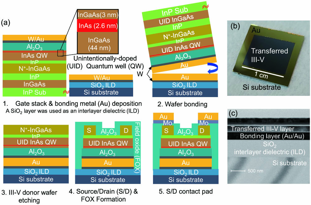
The fabrication process for the InAs QW photo-FET is illustrated in Fig. 1. The III-V stacks, which consist of an unintentionally doped (UID) indium phosphide (InP) seed layer (50 nm), a etching stop layer (200 nm), a UID-InP buffer layer (50 nm), a heavily doped -InGaAs source/drain (S/D) layer (50 nm) with a Si concentration of , and UID-InGaAs (44 nm)/InAs (2.6 nm)/InGaAs (3 nm) quantum well (QW) channel were grown on an InP (001) substrate by molecular beam epitaxy. After pretreatment with ammonia () solution for 2 min and ammonium sulfide [] solution for 5 min, 10 nm thick aluminum oxide () film was deposited as a gate insulator by atomic layer deposition using trimethylaluminium [()] and as precursors. Before wafer bonding, the samples were annealed at 300°C for 10 min to prevent void generation [32]. Then, 11 nm thick tungsten (W) and 55 nm thick gold (Au) were deposited on III-V wafers and 300 nm thick silicon dioxide substrates. Here, W is used as the gate metal and Au is adopted for the reflector and bonding metal. We experimentally found that W can play a role in the adhesion layer between Au and layers. After surface activation using argon (Ar) plasma, the two wafers are directly bonded. The bonded samples were pressed with a pressure of at 100°C for 1 h. The InP donor substrate was removed by mechanical polishing and a hydrochloric acid (HCl) solution. The InGaAs etching stop layer and the InP buffer layer were eliminated by selective wet etching processes using mixed solutions with and , respectively. The optical microscope and transmission electron microscopy (TEM) images of a transferred III-V layer on Si substrates using Au/Au metal bonding are presented in Figs. 1(b) and 1(c). Direct wafer bonding enables efficient transfer of the III-V layer onto Si substrates with excellent crystal quality and large scale. Next, the -S/D and recessed channel were formed by selectively etching the -InGaAs layer on the channel region using a 3 nm thick InP etching stop layer. After channel definition, the 3 nm thick InP etching stop layer was also removed by digital etching processes using oxygen () plasma oxidation and a diluted HF solution. Each device was isolated by wet and dry etching processes. The 300-cycle was deposited as field oxide (FOX). A via hole for S/D contacts was etched using a buffered oxide etchant. For S/D contact pads, molybdenum (Mo)/Au films were deposited by electron-beam evaporation. Finally, the samples were annealed at 300°C for 1 min to improve the interface property between FOX and InGaAs as well as the S/D contact resistivity. For comparison, a 50 nm thick InGaAs photo-FET was fabricated with the same process.
Figure 1.(a) Fabrication flow of InAs QW photo-FETs integrated on interlayer dielectric (ILD)/Si substrates using direct wafer bonding techniques. (b) Optical microscope (OM) and (c) TEM images of a transferred III-V layer on Si substrates using Au/Au metal bonding.
Figure 2(a) shows the 3D schematic image of quantum well (InAs QW) photo-FET fabricated on a Si substrate using Au/Au metal bonding, which also plays the role of a metal reflector. Figure 2(d) shows a high-angle annular dark-field scanning transmission electron microscopy image of InAs QW photo-FETs, confirming a clear and flat bonding interface without a void. Thickness of the 110 nm thick Au reflector was carefully determined to maximize the reflectance. Also, we carefully designed the InAs QW structures because they determine the device characteristics, such as the detection range and effective mobility. The bandgap of the InAs QW and its influence on the detection range are modified by the InAs thickness through the quantum confinement effect [33]. First, the InAs thickness of approximately 3 nm is chosen to avoid the lattice relaxation of the InAs layer grown on because it can cause significant leakage current based on trap-assisted tunneling, which cannot be controlled by the gate bias in the FET [34]. Instead of bilayer structures, an ultrathin bottom capping layer with a thickness of approximately 3 nm was used to improve the effective mobility by decreasing the scattering effect in the adjacent MOS interface [29]. Note that the InAs layer should be positioned within the channel region near the MOS interface. An InGaAs top capping layer with a thickness of around 44 nm was employed to achieve a fully depleted channel and match the channel thickness of reference InGaAs photo-FETs. Figure 2(c) shows the high-resolution TEM image of a channel region for the InAs QW photo-FET. The TEM image confirms that the InAs thickness is around 2.6 nm, displaying a defect-free structure. Additionally, the InGaAs bottom capping layer exhibits a thickness of around 2.2 nm, which might have been reduced from its initial thickness while removing a native oxide layer. The design of the gate insulator, with a thickness of approximately 10 nm, is primarily focused on the FET characteristics, including gate capacitance and gate leakage current. However, the thickness of the gate insulator influences the efficiency of light absorption in the InAs QW layer. Further research regarding the thickness is necessary to optimize the efficiency of light absorption in our devices.
Figure 2.(a) Schematic image of an InAs QW photo-FET. (b) High-angle annular dark-field scanning TEM (HAADF-STEM) image of an InAs QW photo-FET, confirming successful selective etching of -InGaAs source/drain (S/D) regions. High-resolution TEM image shows (c) an InAs QW channel. (d) PL spectrum and (e) energy band diagram of InAs QW structures. The band edge values of the conduction band and valence band for compressively strained InAs (s-InAs) were used to calculate the sub-band energies for an electron (E1) and a heavy hole (HH1). (f) Calculated wavelength peak of the InAs QW as a function of the InAs thickness.
We evaluated the optical bandgap of InAs QW through photoluminescence (PL) measurements, as shown in Fig. 1(d). The carriers in the InAs QW were excited by a 532 nm laser with a low power density of , and the PL spectrum was measured by an extended InGaAs photodetector. The extracted wavelength peak of 2.6 nm thick InAs QW from PL measurements is μ. We also calculated the bandgap of InAs QW theoretically. The conduction and valence bands of compressively strained InAs (s-InAs) were obtained based on the model solid theory [35,36]. The material parameters for InAs and InGaAs were used from Ref. [20]. Then, the sub-band energies for the electron (E1) and heavy hole (HH1) were calculated by solving the Schrödinger equations. The calculated energy band diagram of QW structure is plotted in Fig. 1(e), showing good agreement with the PL measurement. We also calculated the bandgap of InAs QW corresponding to the InAs thickness and the critical thickness of InAs grown on obtained from the energy balance model [37], which shows a good agreement with the experimental results [38], in Fig. 1(f). The PL emission wavelength of InAs QW decreases with an increase in the InAs thickness. However, the InAs thickness should be smaller than the critical thickness because the lattice relaxation causes a significant amount of defect in the InAs QW layer. Our calculation result suggests that the maximum wavelength of InAs QW without lattice relaxation can reach up to μ, indicating further room to increase the wavelength range.
The opto-electrical response of the InAs QW and photo-FETs was examined under illumination using a 1.55 μm wavelength optical source. The optical measurement setup, based on confocal microscopy and an IR camera, is illustrated in Fig. 3(a). The large area devices with a channel length/width of 100/100 μm were used for the optical measurement. The spot size of the optical source focused by an objective lens is smaller than the device area. Figure 3(b) presents the characteristics of InAs QW photo-FETs in the dark and under light illumination. The higher drain current was observed under light illumination than that in dark, indicating that the photocurrent is generated under illumination at a 1.55 μm wavelength. We examined the optical power dependence of the photocurrent () for InAs QW and photo-FETs in Figs. 3(c) and 3(d), respectively. The incident optical power () was adjusted from to 50 μW using a variable optical attenuator and measured by an extended InGaAs photodetector. We found that our InAs QW photo-FETs produce a higher photocurrent and responsivity than reference photo-FETs under the same light incidence. The responsivity () at for both devices was extracted from the photocurrent, as shown in Fig. 3(e). The InAs QW photo-FET exhibits high responsivity, which is 1.8 times greater than that of the InGaAs photo-FET, demonstrating its potential for high-performance photodetector applications.
Figure 3.(a) Measurement configuration based on the confocal microscopy. (b) curves of InAs QW photo-FETs in the dark and under light illumination. Photocurrents for (c) InAs QW photo-FETs and (d) reference InGaAs photo-FETs. (e) Responsivity of InAs QW and reference InGaAs photo-FETs. (f) characteristics, (g) characteristics, and (h) transconductance of InAs QW and reference InGaAs photo-FETs. (i) Comparison of effective mobility for both devices.
To elucidate the main reason of this performance enhancement, it is necessary to understand the gain mechanism of photo-FETs. Previous reports have revealed that the photocurrent generation in photo-FET mainly arises from photovoltaic effects under light illumination [39–41], during which electron-hole pairs are generated in the channel of photo-FET. The photogenerated electrons flow to the drain. On the other hand, the photogenerated holes accumulate in the floating InGaAs body, leading to a decrease in the potential barrier [42]. Consequently, the accumulation of holes causes a negative shift of the threshold voltage (). This phenomenon is commonly referred to as “photovoltaic effects” [39,40] or “photo-gating effects” [15,41]. Then, the responsivity can be expressed as Eq. (1) [39]: where is the photocurrent, is the incident light power, is the transconductance defined by (), W/L is the channel width/length, is the effective mobility, is the gate capacitance, and is the drain voltage. Equation (1) suggests that the transport characteristic and threshold voltage shift are important factors for high responsivity in the photo-FET. The electrical characteristics of the junction-less InAs QW photo-FET and the reference homostructure photo-FET with a channel length/width of 100/100 μm were investigated in Figs. 3(f)–3(i). Figures 3(f) and 3(g) present the and characteristics of both devices, respectively, showing a high on/off ratio of and excellent current saturation properties. The low-leakage current of the junction-less InAs QW photo-FET, with an ultrathin body thickness of 50 nm, is comparable with that of InGaAs photo-FETs due to the fully depleted InAs QW channel with suppressed defects generation. The InAs QW photo-FET achieves a higher on-current () than the InGaAs photo-FETs. We also compared the transconductance () of the photo-FETs, which is an important factor not only for analog applications but also for responsivity. Figure 3(h) shows that the InAs QW photo-FET features a larger transconductance of 10.4 S/μm than the InGaAs photo-FET. These improved electrical characteristics with high and are attributed to the introduction of high-mobility InAs QW channel. To evaluate the effective mobility, we obtained the gate-to-channel capacitance () for the InAs QW photo-FET using a precision LCR meter. The parasitic capacitances between the gate and source/drain were removed using different channel-length devices. The ignorable hysteresis and low-frequency dispersion were confirmed, indicating the high MOS interface properties. The capacitance equivalent thickness of a 10 nm thick gate insulator in our device is around 6.1 nm. Figure 3(e) plots the effective electron mobility of the InAs QW and InGaAs photo-FETs. The InAs QW photo-FET achieves high effective mobility of at a surface concentration of , which is 2.6 times greater than for the photo-FET and even comparable with that of the InAs NW photo-FETs [25–28]. These outstanding electrical characteristics of the InAs QW photo-FET, particularly its enhanced effective mobility, contribute to improving responsivity. This enhanced responsivity of InAs photo-FETs is highly advantageous for applications requiring the detection of low-intensity light.
Equation (1) clearly reveals that the responsivity of photo-FET is inversely proportional to the channel length. We examined the channel-length dependence on the responsivity of InAs QW photo-FETs under illumination at 1.55 μm wavelength. Figures 4(a) and 4(b) display the photocurrent and responsivity of InAs QW photo-FETs with channel length range from 5 to 100 μm. It was observed that the photocurrent and responsivity increase as the channel length decreases. Notably, the InAs QW photo-FET with a channel length of 5 μm achieves a remarkable responsivity of 75,820 A/W at a low optical power of 0.5 nW, as shown in Fig. 4(c). Further enhancement in responsivity can be achieved by scaling down the device dimensions. The improved responsivity achieved through the high effective mobility of the InAs QW photo-FET is expected to be maintained even in short channel devices because the performance of FETs generally follows the scaling rules established for transistor technology. However, it is important to note that short-channel devices require a larger area for source/drain regions. The minimum size of source/drain regions is determined by the contact resistivity between -InGaAs and contact metals. Therefore, the optimal channel length should be determined by considering not only device performance but also a fill factor.
Figure 4.(a) Photocurrent and (b) responsivity for the InAs QW photo-FET with various channel lengths. (c) Relationship between the responsivity and channel length for the InAs QW photo-FET under the low optical power of 0.5 nW.
The time response of the InAs QW photo-FET with a 5 μm channel length was examined using an oscilloscope and a resistor, as illustrated in Fig. 5(a). We added a 100-Ω resistor to the InAs photo-FET and applied a 1 V to the drain. Light illumination is modulated with a frequency of 250 Hz and rising/falling times of 400/400 ns. When the photo-FET is illuminated, the channel conductance decreases, causing a slight change in the voltage division between the photo-FET channel and the resistor. To capture the voltage change, we measured it at the resistor using an oscilloscope. Figure 5(b) shows the transient optical responses of InAs QW photo-FETs at different gate biases of and 0.6 V. Figure 5(c) indicates that the falling time of the InAs QW photo-FET increases exponentially with the gate voltage (), while the rising time is nearly constant. The -dependent falling time is due to the different photocurrent generation mechanisms between on and off states [40]. Figures 5(d) and 5(e) show characteristics and energy band diagrams of the InAs QW photo-FET under illumination and in the dark. When the photo-FET is turned off (off-state), the photogenerated carriers induce the photocurrent, which is referred to as “photoconductive effect.” The fast carrier recombination processes determine the falling time of the optical response in the off-state. On the other hand, when the photo-FET is turned on, the photogenerated holes accumulate in the floated body and cause a threshold voltage shift, resulting in large gain and responsivity. The long falling times in the on-state are due to the relaxation time required for the accumulated holes to disappear. Figure 5(f) shows a responsivity as a function of the gate voltage for the InAs QW photo-FET. The photoconductive effect provides a small responsivity. Therefore, a trade-off relationship exists between the optical response time and responsivity for the InAs QW photo-FET. Our device offers dual-functionality, allowing it to operate in either high responsivity or high-speed mode. Further, it is also important to note that the rising and falling times of 9.1/115 μs in the high responsivity mode of InAs QW photo-FETs are still faster than for charge-trapping-based photo-FETs [27,28].
Figure 5.(a) Schematic image of the time response measurement. (b) Time response for the InAs QW photo-FET at the different of and 0.6 V. (c) The rising and falling time as a function of . (d) characteristics of 5 μm gate length InAs QW photo-FET under illumination and in the dark. (e) The band diagram to explain the photocurrent generation for the InAs QW photo-FET. (f) Responsivity of 5 μm gate length InAs QW photo-FET.
Figure 6.(a) Photocurrent and (b) responsivity of InAs QW photo-FETs under 1.3, 1.55, and 2 μm wavelength optical sources. (c) Benchmark of responsivity of our InAs QW photo-FETs with commercialized InGaAs and extended InGaAs photodiodes (PDs) and InGaAs and InAs NW photo-FETs and PD.
The high responsivity and extended detection range SWIR photo-FET based on the quantum well (InAs QW) channel has been successfully demonstrated on a Si substrate using M3D integration technology. The InAs QW photo-FET shows the high on/off ratio of and the high effective mobility of . Thanks to the improved transport characteristics, the InAs QW photo-FET exhibits 1.8 times higher responsivity than that of the InGaAs homostructure photo-FET and achieves the remarkable value of up to 75,820 A/W at a 1.55 μm wavelength. The InAs QW photo-FETs also demonstrate the fast rising and falling times of 9.1 and 115 μs, respectively. Additionally, the smaller bandgap of InAs QW channel allows for detection of the long-wavelength SWIR near 2 μm.
To further enhance the performance of the InAs QW photo-FET, the following approaches may be promising. One such approach is the utilization of a multilayer quantum well (MQW) structure, which can improve absorption efficiency. However, the MQW can potentially induce side effects in the photo-FET, such as a significant leakage current flowing via the second and higher InAs layers, as the gate controls the carriers near the MOS interfaces. To mitigate these issues, advanced gate geometries and channel structures that enhance gate controllability are necessary for MQW structure photo-FETs. Additionally, scaling down the channel length can enhance the threshold voltage shift by enabling better control of the potential barrier at the narrowed barrier width, leading to a significant reduction in dark current.
Overall, these findings suggest that the InAs QW photo-FET fabricated on Si substrate is promising for high responsivity and broadband SWIR photodetector applications.
[11] S. Manda, R. Matsumoto, S. Saito, S. Maruyama, H. Minari, T. Hirano, T. Takachi, N. Fujii, Y. Yamamoto, Y. Zaizen, T. Hirano, H. Iwamoto. High-definition visible-SWIR InGaAs image sensor using Cu-Cu bonding of III-V to silicon wafer. IEEE International Electron Device Meeting, 390-393(2020).