• Journal of Radiation Research and Radiation Processing
  • Vol. 40, Issue 5, 050701 (2022)
Fei CHU1、2、*, Hongzhuan CHEN1, Ling PENG2, Ying WANG2, and Jingyi NING2
Author Affiliations
  • 1Nanjing University of Aeronautics and Astronautics, Nanjing 211106, China
  • 2Beijing Microelectronics Technology Institute, Beijing 100076, China
  • show less
    DOI: 10.11889/j.1000-3436.2022-0035 Cite this Article
    Fei CHU, Hongzhuan CHEN, Ling PENG, Ying WANG, Jingyi NING. Research and design of high voltage radiation hardened lateral diffused metal oxide semiconductor[J]. Journal of Radiation Research and Radiation Processing, 2022, 40(5): 050701 Copy Citation Text show less
    The schematic diagram of SEB and SEGR in LDMOS
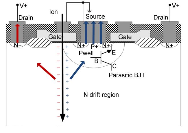
    Fig. 1. The schematic diagram of SEB and SEGR in LDMOS
    Structure of radiation hardened LDMOS
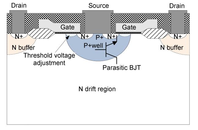
    Fig. 2. Structure of radiation hardened LDMOS
    Transfer characteristic and breakdown characteristic of LDMOS
    Fig. 3. Transfer characteristic and breakdown characteristic of LDMOS
    Diagram of LDMOS SEE irradiation test
    Fig. 4. Diagram of LDMOS SEE irradiation test
    Results of LDMOS SEE irradiation test
    Fig. 5. Results of LDMOS SEE irradiation test
    Micrograph of non-hardened LDMOS SEB failure point
    Fig. 6. Micrograph of non-hardened LDMOS SEB failure point
    Influence of Pwell doping concentration on LDMOS SEB voltage
    Fig. 7. Influence of Pwell doping concentration on LDMOS SEB voltage
    Influence of Pwell doping concentration on LDMOS breakdown characteristic
    Fig. 8. Influence of Pwell doping concentration on LDMOS breakdown characteristic
    LDMOS drain region electric field during SEE
    Fig. 9. LDMOS drain region electric field during SEE
    SEB simulation of non-hardened LDMOS
    Fig. 10. SEB simulation of non-hardened LDMOS
    SEB simulation of radiation hardened LDMOS
    Fig. 11. SEB simulation of radiation hardened LDMOS
    Drain current changes of LDMOS during SEE simulation
    Fig. 12. Drain current changes of LDMOS during SEE simulation
    Gate oxide electric field changes of LDMOS during SEE simulation
    Fig. 13. Gate oxide electric field changes of LDMOS during SEE simulation
    加固措施 Hardening measures加固机理 Hardening mechanism

    降低Pwell电阻;增加Pwell长度

    Decrease Pwell resistence; increase Pwell length

    降低寄生BJT电流增益

    Decrease parasitic BJT current gain

    降低Pwell少数载流子寿命;降低源区掺杂浓度

    Decrease minority carrier lifetime in Pwell region;

    decrease source doping Concentration

    降低寄生BJT发射极注入效率

    Decrease parasitic BJT emitter injection efficiency

    增加N漂移区长度

    Increase N drift region length

    提高雪崩击穿电压

    Increase avalanche break-down voltage

    Table 1. Radiation hardened measurements for LDMOS against single event effect (SEE)
    Fei CHU, Hongzhuan CHEN, Ling PENG, Ying WANG, Jingyi NING. Research and design of high voltage radiation hardened lateral diffused metal oxide semiconductor[J]. Journal of Radiation Research and Radiation Processing, 2022, 40(5): 050701
    Download Citation