
Shu Du, Ayiguli·Kasimu, Yutao Zhang, Wurikaixi·Aiyiti. Mechanical Properties of 316L Stainless Steel Lattice Structure Prepared by Selective Laser Melting[J]. Laser & Optoelectronics Progress, 2022, 59(19): 1914005
- Laser & Optoelectronics Progress
- Vol. 59, Issue 19, 1914005 (2022)
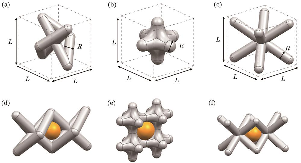
Fig. 1. Lattice structure diagrams. (a) (d) Lattice type A; (b) (e) lattice type B; (c) (f) lattice type C
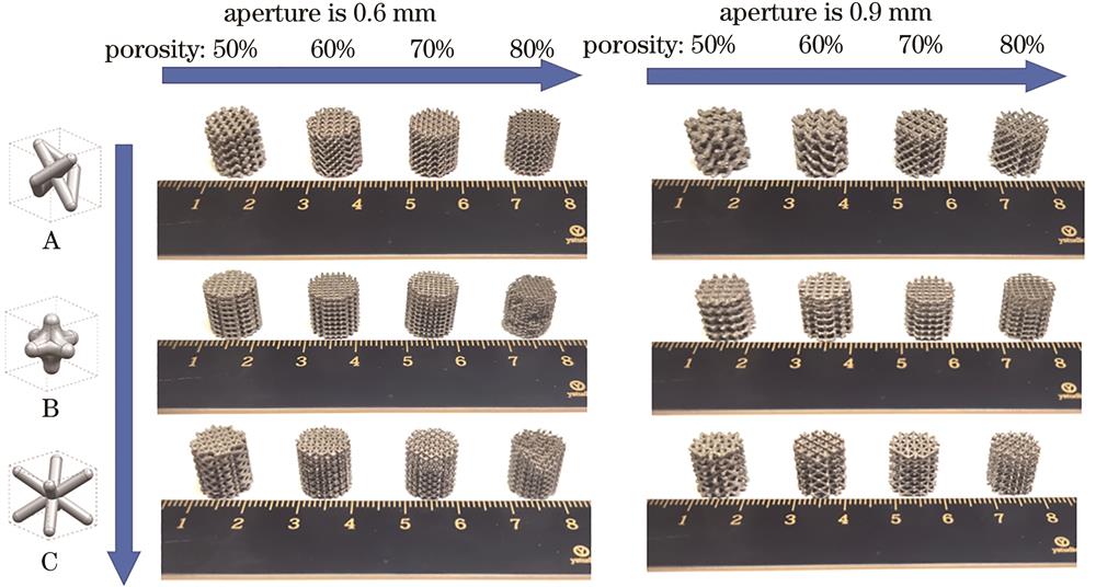
Fig. 2. Lattice structure samples printed by SLM
Fig. 3. Finite element analysis model
Fig. 4. Three types of lattice structure stress-strain curves. (a) Lattice type A; (b) lattice type B; (c) lattice type C
Fig. 5. Change of elastic modulus of lattice structure samples with porosity. (a) Aperture is 0.6 mm; (b) aperture is 0.9 mm
Fig. 6. Change of yield strength of lattice structure samples with porosity. (a) Aperture is 0.6 mm; (b) aperture is 0.9 mm
Fig. 7. Numerical relationship between porosity and elastic modulus of lattice structure. (a) Lattice type A; (b) lattice type B; (c) lattice type C
Fig. 8. Lattice structure stress distributions. (a) Lattice type A; (b) lattice type B; (c) lattice type C
Fig. 9. Lattice structure displacement distributions. (a) Lattice type A; (b) lattice type B; (c) lattice type C
Fig. 10. Deformation mechanism of lattice structure. (a) Lattice type A; (b) lattice type B; (c) lattice type C
Fig. 11. Finite element analysis of deformation mechanism. (a) Lattice type A; (b) lattice type B; (c) lattice type C
Fig. 12. Surface details of lattice structure sample captured by the microscope
Fig. 13. Comparison of rod diameters measured in different directions (top view and side view)
|
Table 1. Design parameters of lattice structure
|
Table 2. Printing defects detected by industrial micro-nano CT system

Set citation alerts for the article
Please enter your email address
© Copyright 2018-2021 | Chinese Laser Press. All Rights Reserved 沪ICP备15018463号-20