Abstract
We demonstrate a novel high-accuracy post-fabrication trimming technique to fine-tune the phase of integrated Mach–Zehnder interferometers, enabling permanent correction of typical fabrication-based phase errors. The effective index change of the optical mode is 0.19 in our measurement, which is approximately an order of magnitude improvement compared to previous work with similar excess optical loss. Our measurement results suggest that a phase accuracy of 0.078 rad was achievable with active feedback control.1. INTRODUCTION
Silicon photonics is a promising technology for monolithic integration of photonic devices and advanced microelectronic circuits in a single chip. It has attracted great interest from both the academic community and industry. A huge amount of resources and effort have been put into silicon photonics research in the last decade.
The Mach–Zehnder interferometer (MZI) is one of the key components for silicon photonics circuits. It is widely used for modulation [1,2], switching [3], filtering, and sensing applications [4]. For most applications, the MZI needs to be working at a particular operating point to achieve optimum performance, where the phase difference between the two arms needs to be fixed. As an example, a symmetrical MZI modulator typically needs to be operated at the quadrature point for the best modulation efficiency [5]. However, this cannot be achieved with current fabrication technologies because of the large phase error between the two MZI arms caused by variations of the fabrication process and wafer properties. Active thermal or electrical tuning is normally required during the operation of the MZI, which consumes substantial additional power and increases the control complexity [5].
Post-fabrication trimming of the optical phase in a waveguide was investigated previously by several groups, primarily for tuning the resonance of ring resonators. Electron-beam (e-beam) induced compaction and strain to the oxide cladding have been proposed to trim the peak resonance of silicon ring resonators [6]. However, the change of the effective index for the optical mode is quite small (around 0.01), which limits the tuning range. E-beam bleaching of a polymer cladding was also proposed for more effective trimming [7]. In addition, ultraviolet (UV) [8] or visible light [9] were also used to tune the silicon microring resonators with polymethyl methacrylate (PMMA) or chalcogenide glass claddings, respectively. However these methods lack universal CMOS compatibility. Surface amorphization and ablation of silicon waveguides with a femtosecond laser were also demonstrated to trim the refractive index [10]. However, it is a rather destructive method with very limited accuracy.
Sign up for Photonics Research TOC. Get the latest issue of Photonics Research delivered right to you!Sign up now
In previous work by Ackert et al. [11], they attempted to apply boron and silicon ion implantation in the silicon waveguide and subsequently trim the refractive index by the thermal annealing process. An effective index change of only 0.02 was achieved, which, however, also induced a 30 dB/mm excess optical loss. In previous work, we have achieved a much higher optical refractive index change [12] with germanium ion implantation at a higher dose, and the excess loss was kept at the same level. However, the whole implanted section was annealed altogether at the same time in the previous work. By adjusting the annealing temperature or laser power, the accuracy and repeatability of the phase trimming process was not satisfactory. There is a threshold effect during the annealing process and the relationship between the refractive index change and either the annealing temperature or the laser power are not linear.
Therefore, in this paper, we propose a novel technique for high-accuracy post-fabrication phase trimming of silicon waveguides, in this case, within an MZI. A section of a Ge implanted silicon waveguide was introduced to each MZI arm. Ge implantation in silicon breaks the chemical bonds and creates amorphous silicon, which has a much higher index than crystalline silicon. The lattice damage density and therefore the refractive index of the implanted region can then be reduced by localized laser annealing. In order to precisely trim the optical phase in the MZI arm, we use a scanning laser to sequentially anneal sections of the implanted waveguide. The optical phase is then controlled accurately by the length of the implanted waveguide that is annealed in each step by the scanning laser. This technique can also be applied to accurately trim the resonance wavelength of ring resonators.
2. DEVICE DESIGN AND LASER ANNEALING
The device design is illustrated in Fig. 1. It was fabricated using silicon-on-insulator (SOI) wafers with a 220 nm top silicon layer and 2 μm buried oxide. All the waveguides for the MZI arms are 500 nm wide with a 100 nm slab. multimode interference (MMI) couplers are used as the optical splitter and combiner of the MZI. The MMI coupler is 44.8 μm long and 6 μm wide. A short taper (20 μm in length) is used to connect the waveguide with the MMI coupler to enhance optical transmission. The devices were formed by a 120 nm dry etch process. Grating couplers were used for light coupling between the devices and optical fibers. Only the TE mode was coupled to the waveguides for characterization. The devices are measured at a wavelength around 1560 nm.
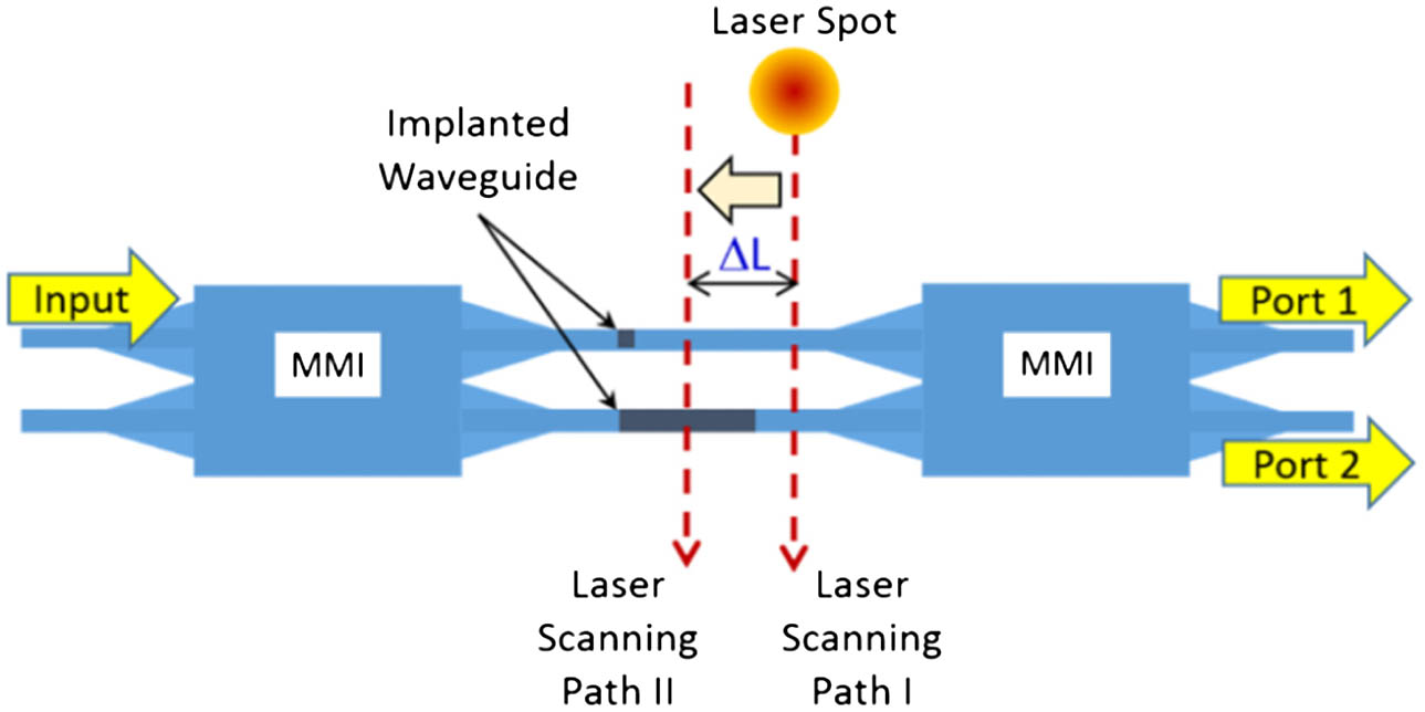
Figure 1.Schematic illustration of the MZI with the Ge implanted waveguides in both arms and the localized annealing process using a scanning laser.
One Ge implanted waveguide section was introduced into each of the MZI arms, as shown in Fig. 1. A longer one (7 μm long) was used for controlling the phase by partial laser annealing. A shorter one (2 μm long) was used to balance the Si/amorphous Si transition loss at the interfaces of both arms. According to our calculation, there is about 1% loss at the interface. After fabrication of the grating couplers and waveguide devices, 20 nm thick plasma-enhanced chemical vapor deposition (PECVD) oxide was deposited as a protective layer. Then an e-beam resist layer was deposited as a mask layer for the Ge implantation. According to our previous results [13], over 80% lattice disorder in silicon would give a refractive index change of 0.5. Ge implantation was carried out with energy of 130 keV and a dose of . The implanted depth is approximately 140 nm into the silicon layer. An optical microscope image of the implanted waveguide sections is shown in Fig. 2.
For the ion implantation process, we have been limited to use ion species that are CMOS compatible. Furthermore, lighter ion species, such hydrogen and oxygen, would not be sufficient to induce enough defects in order to create amorphous silicon. We also want to avoid those ion species that may induce additional free carriers after laser annealing, such as boron. Therefore, Ge ions were used for our project.
The laser annealing setup is shown in Fig. 3. It was designed to deliver 488 nm continuous wave (CW) radiation, emitted by an argon ion laser, to the surface of the silicon chip in a controlled and precise manner. A half-wave plate and a polarization cube splitter were used to adjust the laser power. The laser beam was focused onto the chip surface using a microscope objective lens. and objective lenses were used, which produced spot sizes of 4.7 and 2.5 μm, respectively. The sample was scanned under the laser beam using a set of linear microprecision stages, while a pellicle beam splitter and a CCD camera were used for imaging and control. The scanning speed was 10 μm/s. With successive scans, we gradually increased the annealing length , which ideally corresponds to the length of the implanted waveguide that is annealed.
CW-laser-based annealing has been shown to produce larger silicon crystal grain sizes with fewer defects than those obtained by pulsed laser source systems, resulting in a qualitative improvement in the recrystallization of amorphous silicon for enhanced material quality [14]. It is concluded to be a result of the lower cooling rate after laser irradiation from CW sources. Therefore, a CW laser was used for annealing in this work. The power was set to be constant at 100 mW with the objective lens and 45 mW with the objective lens. This power is chosen because it provides sufficient power density to anneal the Ge implanted silicon material while avoiding damaging the waveguide devices.

Figure 2.Optical microscope image of the Ge implanted waveguides on both arms of the MZI.
Figure 3.Experimental setup for laser annealing (PBS, polarization beam splitter; BS, pellicle beam splitter; MO, microscope objective).
3. EXPERIMENTAL MEASUREMENT RESULTS
Four MZI sample devices (I, II, III, and IV) were tested with the above-mentioned setup. MZI devices I and II were annealed with the objective lens used in the setup. The results are shown in Fig. 4(a) (MZI device I) and Fig. 4(b) (MZI device II). For both MZI devices, we gradually increased the laser annealed length of the implanted waveguide to change the phase difference between the two arms. The position of the laser spot was aligned visually each time after optical measurement. A square shape, as shown in Fig. 2, was used as the alignment mark. We started to record the data (optical transmission) from each port of the MZIs after a first laser scan at position 0 (). Position 0 is defined as the laser spot just touching the end of the implanted region at the right-hand side during scanning, as shown in Fig. 1 (laser scanning path I). Then the annealed length of the implanted waveguide was set at 0.5, 1, 2, 3, and 4 μm sequentially. Therefore, we can tune the phase difference between the two arms of the MZIs.
Figure 4.Measured results (normalized optical transmissions) of the output ports of the (a) MZI device I and (b) MZI device II while changing the annealing length of the implanted waveguide. Calculated results were also fitted and plotted correspondingly. The objective lens was used to anneal these samples.
As shown in Fig. 4, the phase difference between the two arms (characterized by the optical transmission of ports 1 and 2 of the MZIs) was successfully tuned by changing the position of the scanning laser. The quadrature point is achieved at for MZI device I and for MZI device II. We could only achieve an accuracy of approximately 0.5 μm for positioning the laser spot manually by aligning the laser spot to the alignment mark visually on the screen.
In order to improve the accuracy for positioning the laser spot on the chip surface, we used a objective lens in our setup for annealing the MZI devices III and IV. Similar to the testing steps mentioned above, we gradually increased the laser annealed length of the implanted waveguides to change the phase difference between the two arms. The laser spot was smaller and the laser power was reduced to 45 mW in order to maintain a similar power density on the chip surface. More importantly, the image we obtained from the objective lens was two times bigger. Therefore, after the optical measurement, it enabled us to position the laser spot more accurately in reference to the alignment mark and the implanted waveguides. We started to record the data (optical transmission) from each port of the MZIs after a first laser scan at position 0 (). Position 0 is again defined as the laser spot just touching the end of the implanted region at the right-hand side during scanning, as shown in Fig. 1. The laser spot was moved closer to the implanted waveguides because of its smaller diameter. Then the annealed length of the implanted waveguide was increased in steps of 1.0, 2.0, 2.5, 3.0, 3.5, 4.0, 4.5, and 5.0 μm sequentially.
The results are shown in Fig. 5(a) (MZI device III) and Fig. 5(b) (MZI device IV). The phase difference of the two arms (characterized by the optical transmission of ports 1 and 2 of the MZIs) was successfully tuned by changing the position of the scanning laser, with a higher accuracy compared to the previous experimental setup. The quadrature point was achieved at for both MZI devices III and IV. In our measurements, no index change was observed when the laser annealing process was done over the same position of the implanted waveguide for a second time.
Figure 5.Measured results (normalized optical transmissions) of the output ports of the (a) MZI device III and (b) MZI device IV while changing the annealing length of the implanted waveguide. Calculated results were also fitted and plotted correspondingly. The objective lens was used to achieve better position accuracy for laser annealing.
The optical powers and at the two output ports of the MZIs can be estimated by the following equations: where is the overall optical power at the output, and is the phase deference at the output end of the MZI arms, which can be calculated by the following equation: where is the initial phase difference between the two arms after the first laser annealing scan at position 0 () was performed. is a coefficient showing how much phase difference can be changed per micrometer of the implanted waveguide that is annealed.
According to our fitted data, as shown in Figs. 4 and 5, , 3.85, 3.8, and 4.0 rad for MZI devices I, II, III, and IV, respectively. Those devices are from chips diced from a single wafer. Therefore, the variations of the fabrication process and wafer properties are kept to a minimum, yet we still can observe some difference in the initial phase difference between the two arms reinforcing the need for a technique such as this. The coefficient is obtained for all the measured results. The effective index change of the fundamental TE mode can then be calculated by ()
An order of improvement in terms of effective index change was achieved with our post-fabrication trimming technique, as compared to previous results. This result is also consistent with our theoretical prediction. The refractive index of the silicon was increased to 3.96 after Ge ion implantation and then reduced significantly by the laser annealing process [13,15]. The effective index of the optical mode was therefore changed accordingly.
The excess optical loss of the implanted waveguide is mainly associated with the defect concentration in the Si crystal lattice [16,17]. It is possible to reduce the excess loss by decreasing the defect density or reducing the overlap between the defects and the optical mode. However, these methods will also reduce the change of the effective mode index during laser annealing.
The inaccuracy of phase trimming in our measurement has mainly come from the error in manual repositioning of the laser spot after each optical measurement. The laser position is adjusted by hand based on the optical image on a screen before every scan. Better performance can be achieved using an objective lens with higher multiplication for the experimental setup. Besides, more precise trimming is possible with active feedback control, with the optical power of the port monitored while carrying out the laser annealing. Currently, a commercial motor system can typically achieve 100 nm resolution for positioning, which corresponds to an accuracy of 0.078 rad in phase. With this technique, we can fine-tune each device individually to maximize the performance.
4. CONCLUSION
We have demonstrated a practical and accurate post-fabrication trimming technique for silicon integrated MZI devices. Sections of the Ge implanted silicon waveguide were introduced into both arms of an MZI. The Ge implantation into silicon creates amorphous silicon, which has a much higher refractive index than that of crystalline silicon. The refractive index of the amorphous silicon can be reduced by partial annealing with a scanning laser. The optical phase difference between both arms of an MZI can then be precisely controlled by the length of the implanted waveguide that is annealed by the scanning laser. The effective index change of the optical mode is 0.19 in our measurement, which is approximately an order of magnitude improvement compared to previous work [6,11]. A phase accuracy of 0.078 rad is achievable with active feedback control.
Acknowledgment
Acknowledgment. Reed is a Royal Society Wolfson Research Merit Award holder and thanks the Wolfson Foundation and the Royal Society for funding the award. Thomson acknowledges funding from the Royal Society for his University Research Fellowship. The dataset related to this paper is accessible from the University of Southampton (Dataset 1, Ref. [18]).
References
[1] G. T. Reed, G. Mashanovich, F. Y. Gardes, D. J. Thomson. Silicon optical modulators. Nat. Photonics, 4, 518-526(2010).
[2] Z. Yong, S. Shopov, J. C. Mikkelsen, R. Mallard, J. C. C. Mak, S. P. Voinigescu, J. K. S. Poon. Flip-chip integrated silicon Mach–Zehnder modulator with a 28 nm fully depleted silicon-on-insulator CMOS driver. Opt. Express, 25, 6112-6121(2017).
[3] M. R. Watts, J. Sun, C. DeRose, D. C. Trotter, R. W. Young, G. N. Nielson. Adiabatic thermos-optics Mach–Zehnder switch. Opt. Lett., 38, 733-735(2013).
[4] A. Densmore, D.-X. Xu, P. Waldron, S. Janz, P. Cheben, J. Lapointe, A. Delage, B. Lamontagne, J. H. Schmid, E. Post. A silicon-on-insulator photonic wire based evanescent field sensor. IEEE Photon. Technol. Lett., 18, 2520-2522(2006).
[5] D. J. Thomson, H. Porte, B. Goll, D. Knoll, S. Lischke, F. Y. Gardes, Y. Hu, G. T. Reed, H. Zimmermann, L. Zimmermann. Silicon carrier depletion modulator with 10 Gbit/s driver realized in high-performance photonic BiCMOS. Laser Photon. Rev., 8, 180-187(2014).
[6] J. Schrauwen, D. Van Thourhout, R. Baets. Trimming of silicon ring resonator by electron beam induced compaction and strain. Opt. Express, 16, 3738-3743(2008).
[7] S. Prorok, A. Y. Petrov, M. Eich, J. Luo, A. K.-Y. Jen. Trimming of high-Q-factor silicon ring resonators by electron beam bleaching. Opt. Lett., 37, 3114-3116(2012).
[8] L. Zhou, K. Okamoto, S. J. B. Yoo. Athermalizing and trimming of slotted silicon microring resonators with UV-sensitive PMMA upper-cladding. IEEE Photon. Technol. Lett., 21, 1175-1177(2009).
[9] A. A. Canciamilla, F. Morichetti, S. Grillanda, P. Velha, M. Sorel, V. Singh, A. Agarwal, L. C. Kimerling, A. Melloni. Photo-induced trimming of chalcogenide-assisted silicon waveguides. Opt. Express, 20, 15807-15817(2012).
[10] D. Bachman, Z. Chen, R. Fedosejevs, Y. Y. Tsui, V. Van. Permanent fine tuning of silicon microring devices by femtosecond laser surface amorphization and ablation. Opt. Express, 21, 11048-11056(2013).
[11] J. J. Ackert, J. K. Doylend, D. F. Logan, P. E. Jessop, R. Vafaei, L. Chrostowski, A. P. Knights. Defect-mediated resonance shift of silicon-on-insulator racetrack resonators. Opt. Express, 19, 11969-11976(2011).
[12] G. T. Reed, M. M. Milosevic, X. Chen, D. J. Thomson. Trimming of ring resonators via ion implantation in silicon. Proc. SPIE, 10242, 102420Q(2017).
[13] R. Topley, G. Martinez-Jimenez, L. O’Faolain, N. Healy, S. Mailis, D. J. Thomson, F. Y. Gardes, A. C. Peacock, D. N. R. Payne, G. Z. Mashanovich, G. T. Reed. Locally erasable couplers for optical device testing in silicon on insulator. J. Lightwave Technol., 32, 2248-2253(2014).
[14] K. Kitahara, Y. Ohashi, Y. Katoh, A. Hara, N. Sasaki. Submicron-scale characterization of poly-Si thin films crystallized by excimer laser and continuous-wave laser. J. Appl. Phys., 95, 7850-7855(2004).
[15] P. D. Townsend. Optical effects of ion implantation. Rep. Prog. Phys., 50, 501-558(1987).
[16] P. J. Foster, J. K. Doylend, P. Mascher, A. P. Knights, P. G. Goleman. Optical attenuation in defect-engineered silicon rib waveguide. J. Appl. Phys., 99, 073101(2006).
[17] M. J. A. de Dood, A. Polman, T. Zijlstra, E. W. J. M. van der Drift. Amorphous silicon waveguides for microphotonics. J. Appl. Phys., 92, 649-653(2002).
[18] X. Chen, M. Milosevic, D. Thomson, A. Khokhar, Y. Franz, A. Runge, S. Mailis, A. Peacock, G. Reed. Dataset for: Post-fabrication phase trimming of Mach-Zehnder interferometers by laser annealing of germanium implanted waveguides. Univ. Southampton Institutional Repository(2017).


