• Photonics Research
  • Vol. 10, Issue 2, 509 (2022)
Xiaohan Wang1、†, Kunpeng Jia1、3、†,*, Mengwen Chen1, Shanshan Cheng1, Xin Ni1, Jian Guo1, Yihao Li1, Huaying Liu1, Liyun Hao1, Jian Ning1, Gang Zhao1, Xinjie Lv1, Shu-Wei Huang2, Zhenda Xie1、4、*, and Shi-Ning Zhu1
Author Affiliations
  • 1National Laboratory of Solid State Microstructures, School of Electronic Science and Engineering, School of Physics, College of Engineering and Applied Sciences, and Collaborative Innovation Center of Advanced Microstructures, Nanjing University, Nanjing 210093, China
  • 2Department of Electrical, Computer and Energy Engineering, University of Colorado Boulder, Boulder, Colorado 80309, USA
  • 3e-mail: jiakunpeng@nju.edu.cn
  • 4e-mail: xiezhenda@nju.edu.cn
  • show less
    DOI: 10.1364/PRJ.432076 Cite this Article Set citation alerts
    Xiaohan Wang, Kunpeng Jia, Mengwen Chen, Shanshan Cheng, Xin Ni, Jian Guo, Yihao Li, Huaying Liu, Liyun Hao, Jian Ning, Gang Zhao, Xinjie Lv, Shu-Wei Huang, Zhenda Xie, Shi-Ning Zhu. 2 μm optical frequency comb generation via optical parametric oscillation from a lithium niobate optical superlattice box resonator[J]. Photonics Research, 2022, 10(2): 509 Copy Citation Text show less
    Schematic and characterization of an optical superlattice box resonator. (a) Structure of the OSBR. The optical superlattice “box” is sandwiched by lithium tantalate (LT) substrates, with an effective size of 0.484 mm×0.076 mm×48.4 mm. It confines the optical waves for the signal and idler from all six surfaces. (b) Fabrication process of the OSBR. The optical superlattice wafer is thinned to 0.076 mm by mechanical polishing and then sandwiched by LT substrates with Ta2O5 and SiO2 films as buffer layers. Then it is sliced and precisely polished for all the surfaces. Optical coatings are applied with wavelength selectivity: S1, AR at 1048 nm, R=99.8% at 2096 nm; S2, AR at 1048 nm, R=99% at 2096 nm. Finally, the OSBR is mounted in thermally conductive metal housing for thermal control. (c) Measured and simulated FSRs and dispersion of the TM00 mode as a function of wavelength. Small anomalous dispersion is fitted for OSBR at around 2100 nm. (d) OSBR transmission signal. The beam profile is fine adjusted to match the TM00 mode field so that only the TM00 mode can be excited efficiently. The inset is a zoom-in picture of one transmission peak of the TM00 mode with quality factor of 4.0×10⁷.
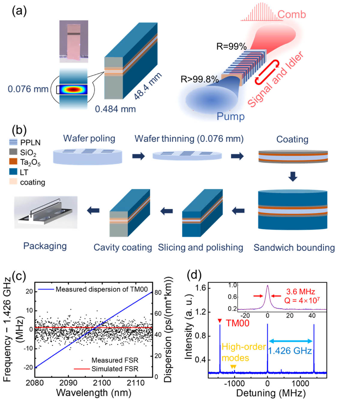
    Fig. 1. Schematic and characterization of an optical superlattice box resonator. (a) Structure of the OSBR. The optical superlattice “box” is sandwiched by lithium tantalate (LT) substrates, with an effective size of 0.484mm×0.076mm×48.4mm. It confines the optical waves for the signal and idler from all six surfaces. (b) Fabrication process of the OSBR. The optical superlattice wafer is thinned to 0.076 mm by mechanical polishing and then sandwiched by LT substrates with Ta2O5 and SiO2 films as buffer layers. Then it is sliced and precisely polished for all the surfaces. Optical coatings are applied with wavelength selectivity: S1, AR at 1048 nm, R=99.8% at 2096 nm; S2, AR at 1048 nm, R=99% at 2096 nm. Finally, the OSBR is mounted in thermally conductive metal housing for thermal control. (c) Measured and simulated FSRs and dispersion of the TM00 mode as a function of wavelength. Small anomalous dispersion is fitted for OSBR at around 2100 nm. (d) OSBR transmission signal. The beam profile is fine adjusted to match the TM00 mode field so that only the TM00 mode can be excited efficiently. The inset is a zoom-in picture of one transmission peak of the TM00 mode with quality factor of 4.0×10⁷.
    Experimental setup and output power tuning measurement of OSBR. (a) Experimental setup for 2 μm OFC generation. TSL, tunable semiconductor laser; YDFA, ytterbium-doped fiber amplifier; CLs, cylindrical lenses; PD, photodetector; BS, beam splitter; PBS, polarization beam splitter; ESA, electronic spectrum analyzer. (b) The output power of the 2 μm OFC as a function of the pump power. The measured maximum output power exceeds 0.34 W with an OPO threshold of 80 mW and a maximum conversion efficiency of 12.4%.
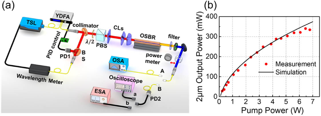
    Fig. 2. Experimental setup and output power tuning measurement of OSBR. (a) Experimental setup for 2 μm OFC generation. TSL, tunable semiconductor laser; YDFA, ytterbium-doped fiber amplifier; CLs, cylindrical lenses; PD, photodetector; BS, beam splitter; PBS, polarization beam splitter; ESA, electronic spectrum analyzer. (b) The output power of the 2 μm OFC as a function of the pump power. The measured maximum output power exceeds 0.34 W with an OPO threshold of 80 mW and a maximum conversion efficiency of 12.4%.
    Study of optical and RF spectra of the 2 μm OFC. (a), (b), (c) The optical spectra of the OFC. The red curves show the measured comb spectra with different pump frequency detuning around 1048 nm and pump power of 6 W. The gray curves show the simulated spectra at stable comb states with 6 W pump power and at −0.6, 4.3, and 11 MHz pump frequency detuning, respectively. The lower panel of (a) is the spectrum in linear scale at −0.6 MHz pump frequency detuning. (d) Map of simulated comb spectra as a function of the pump frequency detuning with 6 W pump power. The highly coherent comb spectrum appears in detuning range from −4 to 0 MHz as a single peak envelope profile; it splits into two peaks at blue detuning, and the separation increases with the detuning. (e) RF beat note spectrum of 2 μm OFC. (f) RF beatnote spectrum around repetition frequency at 1.426 GHz, which shows a clean peak with low noise level. The further zoomed-in result shows a resolution bandwidth (RBW) limited linewidth of 10 Hz (at −3 dB level).
    Fig. 3. Study of optical and RF spectra of the 2 μm OFC. (a), (b), (c) The optical spectra of the OFC. The red curves show the measured comb spectra with different pump frequency detuning around 1048 nm and pump power of 6 W. The gray curves show the simulated spectra at stable comb states with 6 W pump power and at 0.6, 4.3, and 11 MHz pump frequency detuning, respectively. The lower panel of (a) is the spectrum in linear scale at 0.6  MHz pump frequency detuning. (d) Map of simulated comb spectra as a function of the pump frequency detuning with 6 W pump power. The highly coherent comb spectrum appears in detuning range from 4 to 0 MHz as a single peak envelope profile; it splits into two peaks at blue detuning, and the separation increases with the detuning. (e) RF beat note spectrum of 2 μm OFC. (f) RF beatnote spectrum around repetition frequency at 1.426 GHz, which shows a clean peak with low noise level. The further zoomed-in result shows a resolution bandwidth (RBW) limited linewidth of 10 Hz (at 3  dB level).
    Study of temporal waveforms and evolution of the 2 μm χ(2) OFC. (a) The captured temporal waveform of 285 round trips in the time domain. (b) Zoom-in of 10 ns temporal waveform, showing a pulse train with a repetition period of 0.701 ns. (c) Stack plot of 285 round trips within one repetition period, which shows good repeatability with a standard deviation of less than 1.1 %. (d), (e) The simulated pulse train in the time domain within 10 ns and one round trip considering the RF bandwidth limit of the photodetector. They agree well with the experimental results shown in (b) and (c) in comparison, respectively. (f) Temporal evolution simulation for the OFC without RF filtering. A stable temporal pattern is generated after 8000 round trips. The inset of (f) shows a pulse-like temporal waveform in the steady state. (g) The corresponding spectral evolution map. It also shows a stable comb generation. All simulations in (d)–(g) are performed under pump power at 6 W and detuning at −0.6 MHz, for best agreement with the experimental results.
    Fig. 4. Study of temporal waveforms and evolution of the 2 μm χ(2) OFC. (a) The captured temporal waveform of 285 round trips in the time domain. (b) Zoom-in of 10 ns temporal waveform, showing a pulse train with a repetition period of 0.701 ns. (c) Stack plot of 285 round trips within one repetition period, which shows good repeatability with a standard deviation of less than 1.1 %. (d), (e) The simulated pulse train in the time domain within 10 ns and one round trip considering the RF bandwidth limit of the photodetector. They agree well with the experimental results shown in (b) and (c) in comparison, respectively. (f) Temporal evolution simulation for the OFC without RF filtering. A stable temporal pattern is generated after 8000 round trips. The inset of (f) shows a pulse-like temporal waveform in the steady state. (g) The corresponding spectral evolution map. It also shows a stable comb generation. All simulations in (d)–(g) are performed under pump power at 6 W and detuning at 0.6  MHz, for best agreement with the experimental results.
    Numerical modeling of comb generation in OSBR. (a), (b) Maps of simulated temporal deviation of (a) amplitude and (b) phase at different pump power and frequency detuning. (c) Simulated comb spectra at different pump wavelengths. The degenerate wavelength and corresponding GVD are marked in each case. The broadest comb span can be achieved around zero-dispersion wavelength of OSBR.
    Fig. 5. Numerical modeling of comb generation in OSBR. (a), (b) Maps of simulated temporal deviation of (a) amplitude and (b) phase at different pump power and frequency detuning. (c) Simulated comb spectra at different pump wavelengths. The degenerate wavelength and corresponding GVD are marked in each case. The broadest comb span can be achieved around zero-dispersion wavelength of OSBR.
    Xiaohan Wang, Kunpeng Jia, Mengwen Chen, Shanshan Cheng, Xin Ni, Jian Guo, Yihao Li, Huaying Liu, Liyun Hao, Jian Ning, Gang Zhao, Xinjie Lv, Shu-Wei Huang, Zhenda Xie, Shi-Ning Zhu. 2 μm optical frequency comb generation via optical parametric oscillation from a lithium niobate optical superlattice box resonator[J]. Photonics Research, 2022, 10(2): 509
    Download Citation