• Chinese Optics Letters
  • Vol. 19, Issue 9, 092501 (2021)
Linlin Su1、2, Weizong Xu1, Dong Zhou1、*, Fangfang Ren1, Dunjun Chen1, Rong Zhang1, Youdou Zheng1, and Hai Lu1、**
Author Affiliations
  • 1School of Electronic Science and Engineering, Collaborative Innovation Center of Advanced Microstructures, Nanjing University, Nanjing 210023, China
  • 2School of Electronic and Information Engineering, Nanjing University of Information Science & Technology Binjiang College, Wuxi 214105, China
  • show less
    DOI: 10.3788/COL202119.092501 Cite this Article Set citation alerts
    Linlin Su, Weizong Xu, Dong Zhou, Fangfang Ren, Dunjun Chen, Rong Zhang, Youdou Zheng, Hai Lu. Avalanche mechanism analysis of 4H-SiC n-i-p and p-i-n avalanche photodiodes working in Geiger mode[J]. Chinese Optics Letters, 2021, 19(9): 092501 Copy Citation Text show less

    Abstract

    Understanding detailed avalanche mechanisms is critical for design optimization of avalanche photodiodes (APDs). In this work, avalanche characteristics and single photon counting performance of 4H-SiC n-i-p and p-i-n APDs are compared. By studying the evolution of breakdown voltage as a function of incident light wavelength, it is confirmed that at the deep ultraviolet (UV) wavelength region the avalanche events in 4H-SiC n-i-p APDs are mainly induced by hole-initiated ionization, while electron-initiated ionization is the main cause of avalanche breakdown in 4H-SiC p-i-n APDs. Meanwhile, at the same dark count rate, the single photon counting efficiency of n-i-p APDs is considerably higher than that of p-i-n APDs. The higher performance of n-i-p APDs can be explained by the larger impact ionization coefficient of holes in 4H-SiC. In addition, this is the first time, to the best of our knowledge, to report single photon detection performance of vertical 4H-SiC n-i-p-n APDs.

    1. Introduction

    High-sensitivity ultraviolet (UV) detectors are imperative in many key fields, such as non-line-of-sight communication, missile plume detection, environmental monitoring, corona detection, UV astronomical research, and biological molecule detection[13]. Benefiting from high avalanche gain factor, high spectral responsivity, long lifetime, and compact size, the avalanche photodiode (APD) is an attractive candidate to replace conventional photomultipliers in the field of weak UV photon detection[46]. Compared with other wide bandgap semiconductors for UV APD development, 4H-SiC is very competitive, owing to its lower defect density and relatively mature processing technologies[7,8]. 4H-SiC APDs exhibit promising performance, including low dark current, high multiplication gain, and high quantum efficiency (QE).

    Along the wide UV wavelength region ranging from 200 to 400 nm, the solar-blind band (240–280 nm) is what people are mostly interested in, which is due to its ultra-low background noise. In literature, although 4H-SiC APDs with both n-i-p and p-i-n structures have been reported with certain success, there is no detailed avalanche mechanism comparison between the two device structures for deep UV detection[914]. Since deep UV light has short penetration depth in 4H-SiC, photo-carriers are mainly excited in the upper region of the APD structure. Then, electrons and holes would have different drift paths for n-i-p and p-i-n APDs. Considering the fact that the impact ionization coefficient of holes in 4H-SiC is much larger than that of electrons at the same electrical field strength, the performance of n-i-p and p-i-n APDs could be quite different. In this work, 4H-SiC n-i-p and p-i-n APDs are designed and fabricated with similar termination structure and processing technology. A detailed comparison in terms of the avalanche mechanism is conducted. It is determined that due to hole-initiated ionization, n-i-p APDs have better performance for deep UV detection.

    2. Experiment

    The SiC APDs are grown on 4 inch (1 inch = 2.54 cm). n-type 4H-SiC substrates. As shown in Figs. 1(a) and 1(b), the epi-structure of the n-i-p APD from top to bottom consists of a 0.15 µm n+ contact layer (ND=1×1019cm3), a 0.2 µm n transition layer (ND=1×1018cm3), a 0.78 µm n avalanche multiplication layer (ND=1×1015cm3), and a 10 µm p buffer layer (NA=3×1018cm3). Comparatively, the epi-structure of the p-i-n APD consists of a 0.2 µm p+ contact layer (NA=2×1019cm3), a 0.2 µm p transition layer (NA=1×1018cm3), a 0.6 µm p multiplication layer (NA=1×1015cm3), and a 10 µm n buffer layer (ND=3×1018cm3). Figure 1(c) shows the top view image of the fabricated APD. The first step in the fabrication process of both device structures is mesa etching by using inductively coupled plasma etching. In order to enhance the fill factor, the mesa is etched down to the surface of the multiplication layer (∼0.5 µm). In order to prevent mesa edge breakdown, the photoresist reflow technique is employed to obtain a small positive beveled mesa (∼6°)[15,16]. As shown in Fig. 2, the electric field profile of a beveled mesa SiC p-i-n APD is simulated under avalanche breakdown voltage (VB), which indicates that the beveled mesa termination is effective for suppressing the peak electric field around the mesa edge through increasing depletion width. Subsequently, the APD surface is passivated by a thermal oxidation layer and followed by a SiO2 layer deposited by plasma-enhanced chemical vapor deposition (PECVD). Both n and p ohmic contact metals use Ni/Ti/Al/Au deposited by e-beam evaporation, where the thickness of Ni/Ti/Al/Au is 35 nm/50 nm/100 nm/100 nm, respectively. The contact metals are annealed by rapid thermal annealing at 850°C for 3 min in N2 ambient. Finally, the top contact pad based on a Ti/Au bi-layer is deposited by e-beam evaporation. The mesa diameter of both APDs is ∼150 µm, which refers to the top edge of the beveled mesa. Here, it should be noted that the n-i-p APD fabricated by the above process is actually an n-i-p-n diode, in which its avalanche current flows through a forward-biased pn junction formed between the p epi-layer and the n-type substrate. As a result, it is not necessary to expose its p contact layer by deep mesa etching. In a past study, it has been determined that the n-i-p-n APD has similar current-voltage (I-V) and avalanche characteristics to those of conventional n-i-p APDs[17]. The advantage of adopting this n-i-p-n scheme in current work is that both the n-i-p APD and the p-i-n APD under study could be terminated by the same beveled mesa structure, so that similar high fill factors (∼80%) and electrical field modulation effects could be achieved for the two APDs, which is desired for performance comparison.

    Schematic cross section structures of the vertical 4H-SiC (a) n-i-p APD and (b) p-i-n APD; (c) top view image of one fabricated APD.

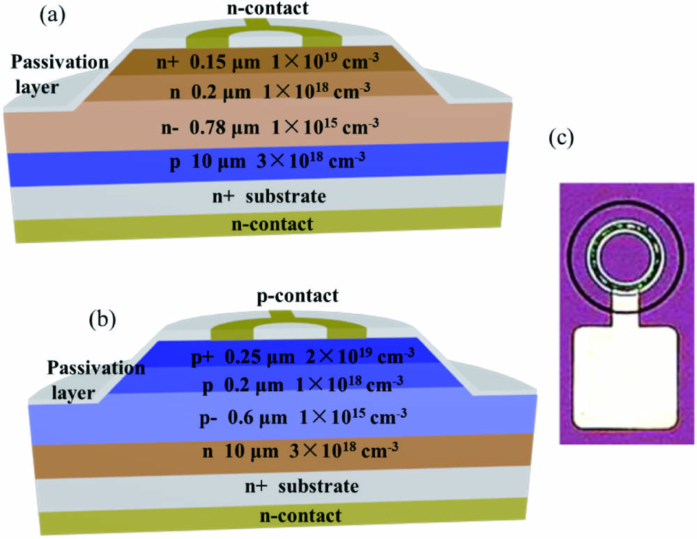
    Figure 1.Schematic cross section structures of the vertical 4H-SiC (a) n-i-p APD and (b) p-i-n APD; (c) top view image of one fabricated APD.

    Simulated 2D electric field distribution of a beveled mesa SiC APD under avalanche breakdown voltage. The inset shows the one-dimensional (1D) electric field profile along the black line marked in the 2D electric field profile.

    Figure 2.Simulated 2D electric field distribution of a beveled mesa SiC APD under avalanche breakdown voltage. The inset shows the one-dimensional (1D) electric field profile along the black line marked in the 2D electric field profile.

    3. Results and Discussion

    Figure 3(a) and 3(b) show the room-temperature (RT) I-V and the gain-voltage curves of the SiC n-i-p and p-i-n APDs, respectively. Both devices exhibit a stable dark current of ∼0.1 pA level before avalanche breakdown occurs. The avalanche gain (M) is calculated by the following equation:M=IMPIMDIPID,where IMP and IMD are the multiplied photo-current and dark current after avalanche multiplication, respectively, while IP and ID are photo-current and dark current before avalanche multiplication, respectively. In this work, IP and ID are measured at 50 V reverse bias. If VB is defined at the multiplication gain of 100, the VB is found at ∼257.5 V and ∼201.2 V for the n-i-p and p-i-n APDs, respectively. At higher overbias, the multiplication gains can reach over 105.

    I-V and gain-voltage curves of (a) the n-i-p APD and (b) the p-i-n APD; the insets show the enlarged gain regions of the two SiC APDs.

    Figure 3.I-V and gain-voltage curves of (a) the n-i-p APD and (b) the p-i-n APD; the insets show the enlarged gain regions of the two SiC APDs.

    In the spectral response measurement, a high-power xenon lamp is used as the light source and a Horiba iHR320 monochromator is employed to sort monochromatic light. A UV-enhanced Si photodiode (Hamamatsu S1226-8BQ) is used to calibrate the incident light power density. The zero-bias spectral response characteristics of two APDs are plotted in Fig. 4, which exhibit similar shape and magnitude. The peak responsivity of the n-i-p APD is ∼0.114 A/W (QE ∼50%) at 285 nm. Comparatively, the p-i-n APD has a maximum QE of ∼48% at 285 nm. The UV/visible (285 nm/400 nm) rejection ratio of both devices is higher than 104. In addition, the overall QE of the p-i-n APD is slightly lower than that of the n-i-p APD over the whole UV wavelength region, which should be caused by its slightly thicker p+ contact layer.

    Zero-bias spectral response curves of n-i-p and p-i-n APDs.

    Figure 4.Zero-bias spectral response curves of n-i-p and p-i-n APDs.

    Next, the single photon detection performance of the n-i-p and p-i-n APDs is compared, which is characterized by a passive quenching circuit [the inset in Fig. 5(a)]. The APDs are biased above VB, and the avalanche events are quenched by a 50 kΩ quenching resistor. The voltage pulse signals are recorded by a high-speed oscilloscope, which is connected with a 100 Ω sampling resistor in parallel. A 265 nm UV LED is used to evaluate the detection capability of devices, and the calibrated incident UV photon flux is 1.2×10⁷ photons/s. A typical avalanche voltage pulse signal is shown in Fig. 5(a). The RT dark count rate (DCR) of the two APDs is shown in Fig. 5(b) as a function of overbias. Since the VB of the two APDs is different due to the small thickness difference of their multiplication layers, here, overbias is intentionally normalized to respective VB for fair comparison. A good exponential dependence of DCR on overbias is observed, which agrees with past reports that trap-assisted tunneling is the main source of DCR in current SiC APDs[18]. The DCR of the n-i-p APD is lower than that of the p-i-n APD. For example, at 1% overbias the DCR of the n-i-p APD is ∼13 kHz, while the DCR of the p-i-n APD is ∼28 kHz. The single photon detection efficiency (SPDE) is calculated by using the following equation:SPDE=PCRDCRn×100%,where n is the total number of incident UV photons of a specific wavelength per second, and PCR is photon count rate. At the same overbias, the SPDE of the n-i-p APD is higher [see Fig. 5(c)]. For example, at 1% overbias, the SPDE of the n-i-p APD is ∼2 times higher than that of the p-i-n APD. With the increase of overbias, the SPDE increases due to the enhanced photo-carrier avalanche multiplication probability at a high electric field. At the same DCR, the SPDE of the n-i-p APD is considerably higher [see Fig. 5(d)], which certainly cannot be explained by the slightly higher zero-bias QE of the n-i-p APD.

    (a) Typical avalanche voltage pulse signal under passive quenching circuit (the inset shows the schematic diagram of passive quenching circuit), (b) the DCR versus normalized overbias curves, (c) the SPDE versus normalized overbias curves, and (d) SPDE versus DCR curves of the n-i-p and p-i-n APDs.

    Figure 5.(a) Typical avalanche voltage pulse signal under passive quenching circuit (the inset shows the schematic diagram of passive quenching circuit), (b) the DCR versus normalized overbias curves, (c) the SPDE versus normalized overbias curves, and (d) SPDE versus DCR curves of the n-i-p and p-i-n APDs.

    The capacitance of the APDs is calculated by the following equation:C=εε0Sd,where ε, ε0, S, and d are relative permittivity, vacuum permittivity, effective area, and depletion layer width of the APD, respectively. Based on this equation, capacitance of the n-i-p and the p-i-n APDs is estimated at ∼1.9 pF and ∼2.5 pF, respectively. The experimental capacitance of the n-i-p and p-i-n APDs is ∼3–4 pF, which is larger than that of the calculated geometric values due to the parasitic effects of measurement cables and probes during on-wafer testing. The time from avalanche onset to avalanche quenching is called the quenching time, which can be calculated by the following equation:Tq(CAPD+Cs)×RAPD.

    The time taken to bring the APD back to its original state is called the reset time, which is calculated by the following equation:Tr=(CAPD+Cs)×RL,where CAPD and Cs are the junction capacitance of the APD and stray capacitance, respectively, while RAPD is the resistance of the APD. RAPD is ∼150 Ω derived from the linear region of the forward I-V curve. From Fig. 5(a), the quenching time and reset time are ∼1 ns and ∼300 ns, respectively, so the stray capacitance of the passive quenching circuit is ∼ 5 pF. During the quenching process of avalanche multiplications, the time during which the APD is not responsive to further incoming photons is called dead time. The dead time includes the avalanche quenching time and the APD reset time. However, when the APD is biased beyond VB, it is able to detect the next photon prior to being fully reset. Thus, apparent fluctuations in the reset waveform can be observed [see Fig. 5(a)].

    To understand the detailed avalanche mechanisms of SiC APDs, the photon-induced multiplication characteristics are measured at various wavelengths ranging from 220 nm to 330 nm. Figures 6(a) and 6(b) show the selected gain-voltage curves of the n-i-p and p-i-n APDs obtained under 260 nm, 280 nm, and 300 nm UV illumination, respectively. It is found that with increasing illumination wavelength, the gain-voltage curves of the n-i-p APD shift towards higher voltage with a corresponding higher VB. Meanwhile, an opposite trend is observed for the p-i-n APD. The detailed evolution behavior of VB as a function of wavelength is summarized in Fig. 6(c). A VB shift up to 2 V can be observed, which is fairly large compared with normal overbias applied during Geiger mode operation.

    Gain-voltage curves measured at 260, 280, and 300 nm illumination for (a) the n-i-p APD and (b) the p-i-n APD. (c) The variation of VB as a function of UV illumination wavelength.

    Figure 6.Gain-voltage curves measured at 260, 280, and 300 nm illumination for (a) the n-i-p APD and (b) the p-i-n APD. (c) The variation of VB as a function of UV illumination wavelength.

    The following physical picture can explain the obvious difference in terms of single photon detection performance and VB shift trend versus wavelength for the two APDs. As illustrated in Fig. 7, electron–hole pairs are mainly excited in the upper region of the depletion layer under front deep UV illumination due to the large absorption coefficient of 4H-SiC for high-energy photons[19]. For n-i-p APDs under reverse bias, most holes would drift across the whole depletion layer towards the p contact layer, having an average long acceleration and multiplication distance. On the other hand, most electrons would be quickly swept back to the n contact layer, having much less chance for impact ionization. Thus, for n-i-p APDs in the deep UV region, the dominated carriers triggering avalanche events are photo-excited holes. At a higher wavelength, the light penetration depth would increase, which leads to more electron–hole pairs being excited in the deeper region of the depletion layer. Then, some electrons would gain enhanced impact ionization probability due to their longer drift and acceleration distance. Therefore, with increasing wavelengths from deep UV to more than 300 nm, the avalanche events gradually vary from dominant hole-initiations to mixed carrier-initiations. The situation of the p-i-n APD is opposite to that of the n-i-p APD. At the deep UV wavelength region, the avalanche events in p-i-n APDs are mainly electron-initiations, while the chance of mixed carrier initiations increases at higher wavelengths. Specifically, according to the simulated absorption spectrum of 4H-SiC, the penetration depths of 240 nm and 300 nm UV light are ∼50 nm and ∼2.5 µm, respectively[19]. Thus, under 240 nm UV illumination, the avalanche events in SiC n-i-p APDs should be mainly hole-initiations, while the dominated mechanism for avalanche multiplications in SiC p-i-n APDs is the electron-initiation. As the UV wavelength increases to 300 nm, avalanche events in both types of APDs should be mixed carrier-initiations. Considering the fact that the ionization coefficient of holes in 4H-SiC is considerably larger than that of electrons[2023], dominant hole initiation means smaller critical electric field and higher gain factor. Because of this, the gain-voltage curves are strongly UV wavelength dependent. In addition, the lower critical electric field also explains why the n-i-p APD with dominant hole-initiated avalanche multiplications has lower DCR.

    Schematics of the carrier ionization process at different incident light wavelengths for (a) the n-i-p APD and (b) the p-i-n APD. The illumination wavelength varies from deep UV to near UV wavelength regions.

    Figure 7.Schematics of the carrier ionization process at different incident light wavelengths for (a) the n-i-p APD and (b) the p-i-n APD. The illumination wavelength varies from deep UV to near UV wavelength regions.

    4. Conclusions

    In summary, vertical Geiger mode 4H-SiC n-i-p and p-i-n APDs have been fabricated and characterized. The n-i-p APD exhibits an overall better single photon counting performance for deep UV detection, which can be explained by its dominant hole-initiated avalanche characteristics. Comparatively, the avalanche events in p-i-n APDs are mainly electron-initiations in the deep UV wavelength region. Since the impact ionization coefficient ratio of holes to electrons is much larger than one, 4H-SiC APDs with dominant hole-initiated avalanche would feature relatively lower critical electric field strength and then fewer dark counts. In addition, this is the first time, to the best of our knowledge, to report single photon detection characteristics of vertical SiC n-i-p-n APDs with an enhanced fill factor.

    References

    [1] H. Chen, K. Liu, L. Hu, A. A. Al-Ghamdi, X. Fang. New concept ultraviolet photodetectors. Mater. Today, 18, 493(2015).

    [2] Y. Wang, Y. Qian, X. Kong. Photon counting based on solar-blind ultraviolet intensified complementary metal-oxide-semiconductor (ICMOS) for corona detection. IEEE Photon. J., 10, 7000919(2018).

    [3] R. H. Hadfield. Single-photon detectors for optical quantum information applications. Nat. Photon., 3, 696(2009).

    [4] X. Yi, S. Xie, B. Liang, L. W. Lim, J. S. Cheong, M. C. Debnath, D. L. Huffaker, C. H. Tan, J. P. R. David. Extremely low excess noise and high sensitivity AlAs0.56Sb0.44 avalanche photodiodes. Nat. Photon., 13, 683(2019).

    [5] J. C. Campbell. Recent advances in avalanche photodiodes. J. Lightwave Technol., 34, 278(2016).

    [6] C. J. Chunnilall, I. P. Degiovanni, S. Kueck, I. Müller, A. G. Sinclair. Metrology of single-photon sources and detectors: a review. Opt. Eng., 53, 1910(2014).

    [7] A. Vert, S. Soloviev, P. Sandvik. SiC avalanche photodiodes and photomultipliers for ultraviolet and solar-blind light detection. Phys. Status Solidi A, 206, 2468(2009).

    [8] A. R. Powell, L. B. Rowland. SiC materials-progress, status, and potential roadblocks. Proc. IEEE, 90, 942(2002).

    [9] X. Bai, H. Liu, D. C. Mcintosh, J. C. Campbell. High-detectivity and high-single-photon-detection-efficiency 4H-SiC avalanche photodiodes. IEEE J. Quantum Electron., 45, 300(2009).

    [10] D. Zhou, F. Liu, H. Lu, D. Chen, F. Ren, R. Zhang, Y. Zheng. High-temperature single photon detection performance of 4H-SiC avalanche photodiodes. IEEE Photon. Technol. Lett, 26, 1136(2014).

    [11] X. Guo, A. L. Beck, Z. Huang, N. Duan, J. C. Campbell, D. Emerson, J. J. Sumakeris. Performance of low-dark-current 4H-SiC avalanche photodiodes with thin multiplication layer. IEEE Trans. Electron Devices, 53, 2259(2006).

    [12] J. Hu, X. Xin, X. Li, J. H. Zhao, B. L. VanMil, K. K. Lew, R. L. Myers-Ward, C. R. Eddy, D. K. Gaskill. 4H-SiC visible-blind single-photon avalanche diode for ultraviolet detection at 280 and 350 nm. IEEE Trans. Electron Devices, 55, 1977(2008).

    [13] X. Y. Zhou, J. Li, W. L. Lu, Y. Wang, X. Song, S. Yin, X. Tan, Y. Lü, H. Guo, G. Gu, Z. Feng. Large-area 4H-SiC avalanche photodiodes with high gain and low dark current for visible-blind ultraviolet detection. Chin. Opt. Lett., 16, 060401(2018).

    [14] X. Y. Zhou, X. Tan, Y. Wang, X. Song, T. Han, J. Li, W. Lu, G. Gu, S. Liang, Y. Lü, Z. Feng. High-performance 4H-SiC p-i-n ultraviolet avalanche photodiodes with large active area. Chin. Opt. Lett., 17, 090401(2019).

    [15] A. L. Beck, B. Yang, X. Guo, J. C. Campbell. Edge breakdown in 4H-SiC avalanche photodiodes. IEEE J. Quantum Electron., 40, 321(2004).

    [16] X. Guo, A. L. Beck, J. C. Campbell, D. Emerson, J. Sumakeris. Spatial nonuniformity of 4H-SiC avalanche photodiodes at high gain. IEEE J. Quantum Electron., 41, 1213(2005).

    [17] X. Cai, L. Li, H. Lu, D. Zhou, W. Xu, D. Chen, F. Ren, R. Zhang, Y. Zheng, G. Li. Vertical 4H-SiC n-i-p-n APDs with partial trench isolation. IEEE Photon. Technol. Lett, 30, 805(2018).

    [18] S. Yang, D. Zhou, X. Cai, W. Xu, H. Lu, D. Chen, F. Ren, R. Zhang, Y. Zheng, R. Wang. Analysis of dark count mechanisms of 4H-SiC ultraviolet avalanche photodiodes working in Geiger mode. IEEE Trans. Electron Devices, 64, 4532(2017).

    [19] H. Y. Cha, P. M. Sandvik. Electrical and optical modeling of 4H-SiC avalanche photodiodes. Jpn. J. Appl. Phys., 47, 5423(2008).

    [20] T. Hatakeyama, T. Watanabe, T. Shinohe, K. Kojima, K. Arai, N. Sano. Impact ionization coefficients of 4H silicon carbide. Appl. Phys. Lett., 85, 1380(2004).

    [21] J. E. Green, W. S. Loh, A. R. J. Marshall, R. C. Tozer, J. P. R. David, S. I. Soloviev, P. M. Sandvik. Impact ionization coefficients in 4H-SiC by ultralow excess noise measurement. IEEE Trans. Electron Devices, 59, 1030(2012).

    [22] M. Hjelm, H. Nilsson, A. Martinez, K. F. Brennan, E. Bellotti. Monte Carlo study of high-field carrier transport in 4H-SiC including band-to-band tunneling. J. Appl. Phys., 93, 1099(2003).

    [23] H. Niwa. Impact ionization coefficients in 4H-SiC toward ultrahigh-voltage power devices. IEEE Trans. Electron Devices, 62, 3326(2015).

    Linlin Su, Weizong Xu, Dong Zhou, Fangfang Ren, Dunjun Chen, Rong Zhang, Youdou Zheng, Hai Lu. Avalanche mechanism analysis of 4H-SiC n-i-p and p-i-n avalanche photodiodes working in Geiger mode[J]. Chinese Optics Letters, 2021, 19(9): 092501
    Download Citation