
Hao Zhang, Qiangsheng Cui, Xu Yan, Jiahui Shi, Fujiang Lin. A 0.5–3.0 GHz SP4T RF switch with improved body self-biasing technique in 130-nm SOI CMOS[J]. Journal of Semiconductors, 2020, 41(10): 102404
- Journal of Semiconductors
- Vol. 41, Issue 10, 102404 (2020)
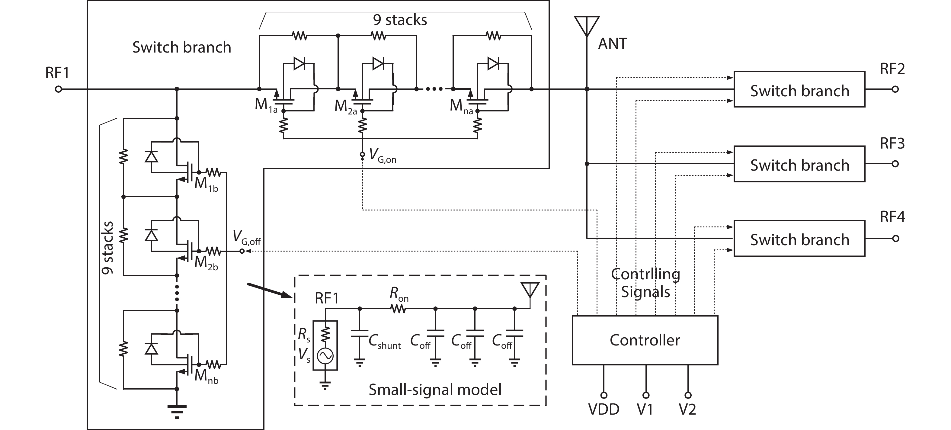
Fig. 1. The block diagram of the proposed SP4T switch. Schematic of a single switch branch is depicted.
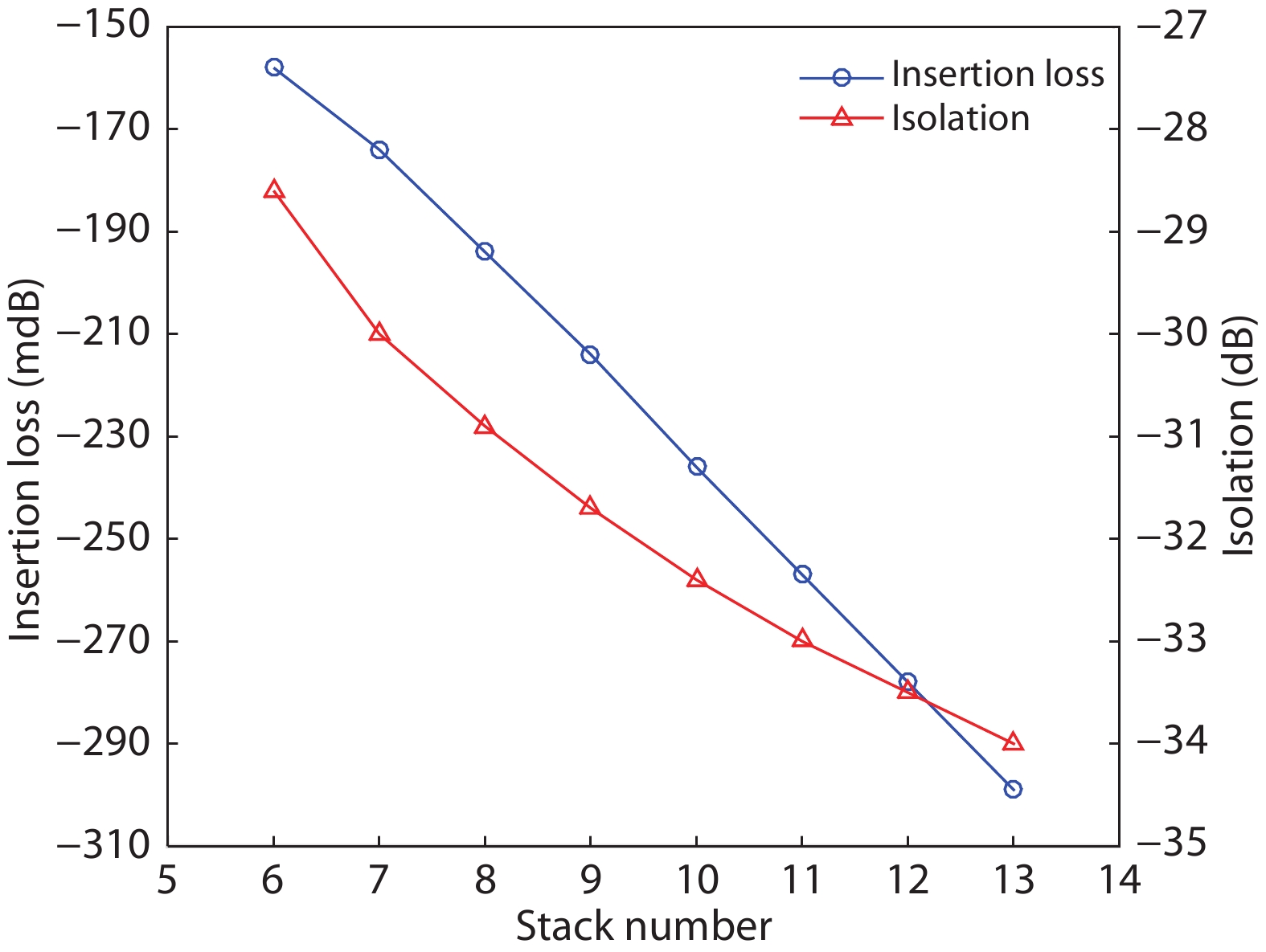
Fig. 2. (Color online) IL and isolation at 1.98 GHz vs stack number.
Fig. 3. Input 0.1-dB compression point at 1.9 GHz vs. stack number.
Fig. 4. (Color online) IL and isolation vs series-FET width.
Fig. 5. Different biasing strategies. (a) Floating body FET biasing. (b) Resistive body-floating biasing. (c) DC-lifting biasing. (d) Proposed body self-biasing strategy using diodes.
Fig. 6. (Color online) IL and isolation of different biasing strategies.
Fig. 7. (Color online) Harmonic level at 1.98 GHz of different biasing strategies.
Fig. 8. Block diagram of the controller.
Fig. 9. (Color online) Micrographs of the fabricated chip and evaluation board.
Fig. 10. (Color online) Measured insertion loss of the SP4T switch.
Fig. 11. (Color online) Measured isolation of the proposed SP4T switch.
Fig. 12. Simulated input power compression point of the SP4T switch.
Fig. 13. Measured input power compression point of the SP4T switch.
Fig. 14. (Color online) Measured 2nd harmonics of the SP4T switch.
Fig. 15. (Color online) Measured 3rd harmonics of the SP4T switch.
|
Table 1. P 0.1 dB at 1.9 GHz of different biasing strategies.
| ||||||||||||||||||||||||||||||||||||||||||||||||||||||||||||||||||||||||||||||
Table 2. Comparison of RF switch performance.


Set citation alerts for the article
Please enter your email address

© Copyright 2018-2021 | Chinese Laser Press. All Rights Reserved 沪ICP备15018463号-20