
Xizheng Ke, Kena Han. Wavefront Simulation and Wavefront Correction of Liquid Crystal Spatial Light Modulator[J]. Laser & Optoelectronics Progress, 2019, 56(5): 051403
- Laser & Optoelectronics Progress
- Vol. 56, Issue 5, 051403 (2019)
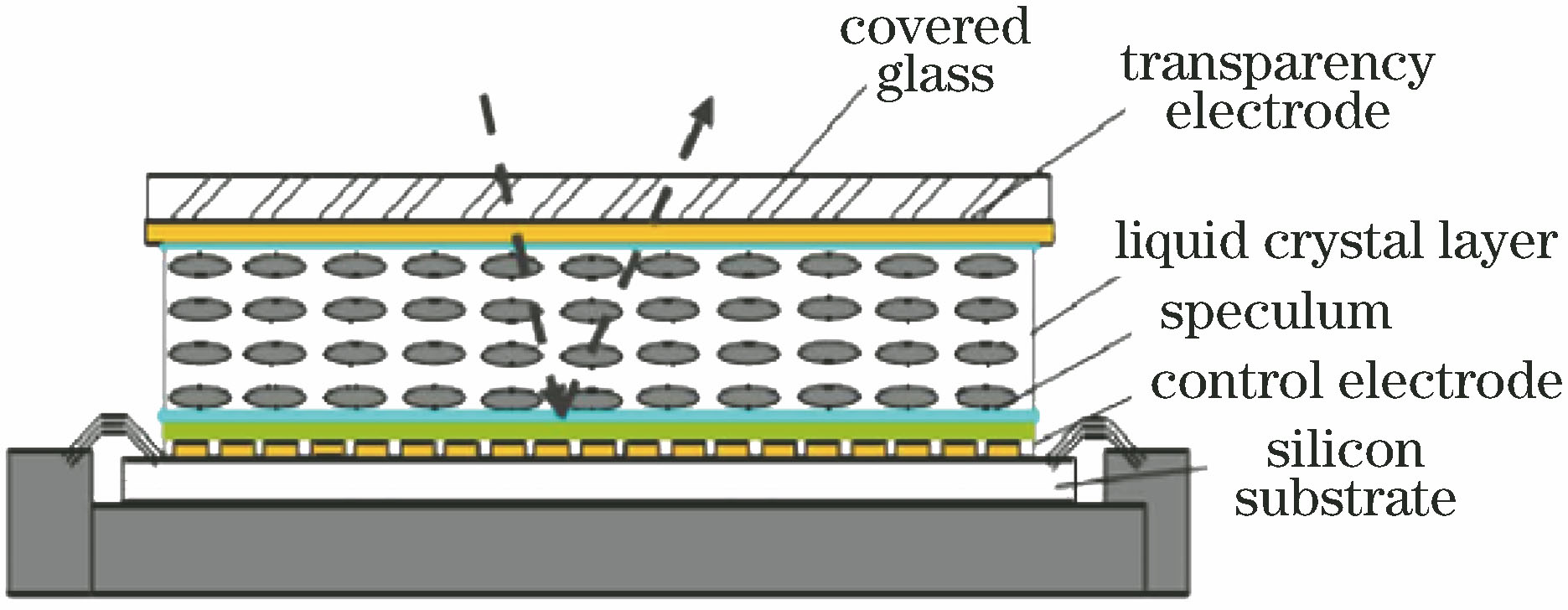
Fig. 1. Structure of reflective LC-SLM
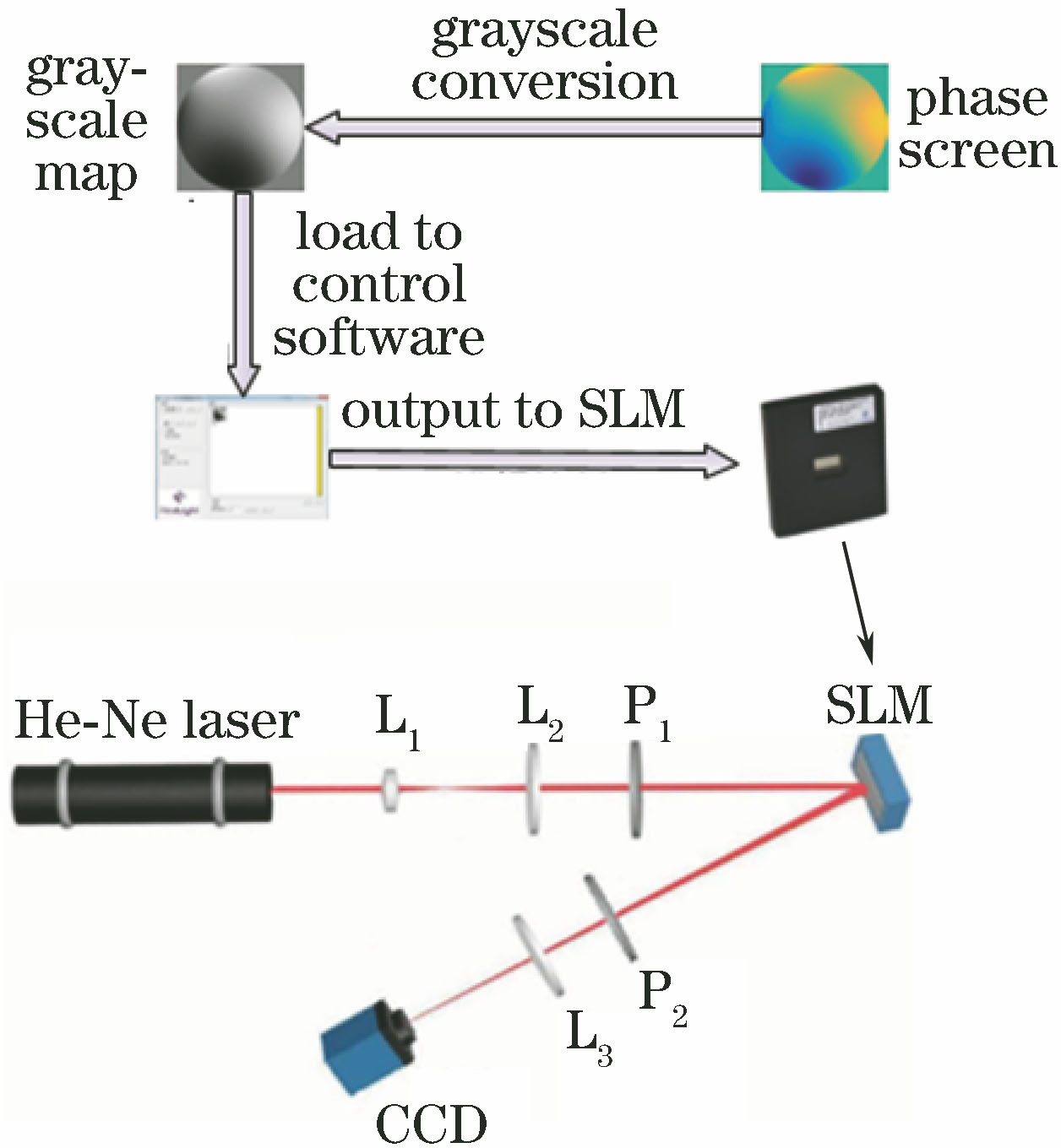
Fig. 2. LC-SLM grayscale image loading and wavefront simulation diagram
Fig. 3. Schematic of wavefront conjugation
Fig. 4. Distorted and corrected spot simulation. (a) Three-dimensional image and (b) two-dimensional grayscale image of distorted spot; (c) three-dimensional image and (d) two-dimensional grayscale image of corrected spot
Fig. 5. Schematic of static wavefront correction using wavefront conjugation
Fig. 6. Optical path diagram of phase modulation experiment of SLM
Fig. 7. Phase modulation experimental process of SLM. (a) Image A; (b) phase diagram of image A; (c) SLM modulated image collected by CCD
Fig. 8. Experimental optical path for wavefront simulation and wavefront correction by LC-SLM
Fig. 9. Phase screen and distortion waveform for wavefront simulation. (a) 15th order Zenick phase screen grayscale image; (b) three-dimensional wavefront map of distorted wavefront
Fig. 10. Spot pattern collected by CCD. (a) Initial spot; (b) distorted spot; (c) corrected spot
|
Table 1. Device parameters of spatial light modulator

Set citation alerts for the article
Please enter your email address
© Copyright 2018-2021 | Chinese Laser Press. All Rights Reserved 沪ICP备15018463号-20