Abstract
We propose a beam reconfigurable micro-strip quasi-Yagi-Uda (QYU) antenna operating at terahertz (THz) frequencies. The antenna, on a metal-backed SiO2 substrate, consists of a metallic micro-strip transmission line, a metallic reflector, a metallic half-round micro patch, and three groups of monolayer-graphene-patch directors. Because the conductivities of the graphene patches can be electrically tuned, the radiation direction of the QYU antenna can be dynamically controlled by adjusting the bias voltages applied to the graphene patches. The basic properties and the tunable behaviors of the antenna are systemically simulated and optimized. It has very fast modulation speed and very low return loss. In particular, the numerical results show that the main radiation lobe angle φ (azimuth angle) of the QYU antenna can be swept from 30° to 150° in θ=60° (zenith angle) plane with different configurations of bias voltages applied to the graphene-patch directors. The proposed antenna is very suitable for THz beam reconfigurable applications, such as phased array radar systems.Introduction
The beam reconfigurable antennas have attracted growing interests, the beam directivities and the radiation patterns of which can be dynamically changed according to demand. Such antennas have the potentials to avoid noise sources, provide larger coverage by steering the angle of the main lobe, and improve the beam steering capability [1,2]. The reconfigurability of beam directivity is a frontier subject in the field of antennas. The beam reconfigurable antennas can be exploited in the multiple-input-multiple-output (MIMO) systems to increase the system capacity [3]. And such antennas are compatible with micro-strip-based monolithic-microwave integrated-circuit (MMIC), which are useful to improve the performance of MMIC. Traditionally, the ways to realize reconfigurable antennas are mostly to load high-frequency electronic devices and use mechanical methods to adjust the antenna structures, which are complicated in structure, frequency limited, and inefficient [1]. Graphene, as the first truly two-dimensional material, has unique thermal, mechanical, optical, and electrical properties [4,5,6,7]. Among all these interesting properties, the bias-voltage-tunable optical conductivity covering the THz band is very useful for providing an effective way to realize real-time electrically reconfigurable THz antennas.
In recent years, many investigations have been performed in the research of graphene-based reconfigurable THz antennas and a series of progress has been achieved. Dragoman et al. designed a graphene-based THz dipole antenna and confirmed that the radiation characteristics can be controlled by applying a bias voltage to graphene[8]. Llatser et al. proposed a graphene nano-patch antenna and systematically analyzed its THz radiation characteristics[9]. Huang et al. proposed a switchable high-impedance surface (HIS) based on single-layer graphene and designed a radiation pattern reconfigurable THz antenna based on such a switchable HIS [10]. Zheng et al. proposed a reconfigurable MIMO system using graphene nano-patch antennas[11]. Wu et al. designed a graphene-based Yagi-Uda antenna with reconfigurable radiation patterns[12]. However, these antennas are not very good at steering the angle of the THz beam due to the limited steering angle and the low radiation efficiency.
The Yagi-Uda antenna was first reported in 1928[13]. Because of the feature characteristics, such as end-fire radiating pattern and simple structure, the Yagi-Uda antennas have been used to design the beam reconfigurable antennas [14,15,16,17]. Several approaches for achieving the reconfigurability of antenna are through micro-strip Yagi-Uda antennas [18], which we refer to as quasi-Yagi-Uda (QYU) antennas. In general, a QYU antenna is composed of several patches (one driven element, one reflector, and one or more directors) that are electromagnetically coupled to one another to steer the angle of the main lobe.
In this paper, a type of graphene-based beam reconfigurable QYU antennas working at THz frequencies is proposed. Graphene patches are used to replace the metallic parasitic elements in the conventional Yagi-Uda antenna, and the patches are divided into three groups, each of which is as a director. Because the complex conductivity of graphene can be tuned by applying different bias voltages, by switching the states of different group of graphene-patch directors, the graphene patches can be operated as directors or not, and the function of sending (receiving) signals only toward (from) the target direction is achieved. When bias voltages are applied to different graphene-patch directors, the beam direction of the proposed device can be scanned in the wide-angle (azimuth angle φ) range of 30°-150° in zenith angle θ=60° plane. Moreover, it has very fast modulation speed, low return loss, and high radiation efficiency.
1 Tunability of graphene optical conductivity
Graphene is a two-dimensional material composed of one layer of carbon atoms with a two-dimensional honeycomb lattice structure, which was first obtained in 2004 by Geim and Novoselov [19]. For a single-layer graphene, due to the unique electric band structure of linear energy-momentum dispersion relation near the Dirac cones at the K and K’ points in the first Brillouin zone, the optical conductivity can be written as the sum of the intra-band conductivity σintra and the inter-band conductivity σinter[20,22,23],
and
where e is the electron charge, ω is the angular frequency, KB is the Boltzmann constant, ℏis the reduced Plank constant, T is the temperature in Kelvin, EF is the Fermi energy, µc is the chemical potential, and Γ=1/2τ is the carrier scattering rate with τ the carrier scattering time.
In the microwave, THz, and far-infrared spectral bands, theoretical and experimental investigations show that the optical conductivity of graphene satisfies the widely used Drude model [21,24,25,26,27,28]. And in the THz band, inter-band transitions are prohibited due to insufficient incident photon energy, and intra-band transitions are in the dominant position. Within the framework of Boltzmann transport theory, the intra-band Drude conductivity for single-layer graphene in THz band can be written as [24,26,29],
The Fermi energy EF is a function of carrier concentration N,
where vF is the Fermi velocity, and the positive (negative) sign in the formula represents the electron (hole) doping.
From equations (3) and (4), the intra-band optical conductivity can be controlled by adjusting the Fermi energy (carrier concentration) in graphene. The bipolar electrical doping effect of graphene allows its electron (hole) concentration to be continuously changed up to 1013 cm-2[20,30]. Therefore, a bias voltage can be applied to effectively adjust the carrier concentration and then the optical conductivity of graphene.
2 Simulation and antenna performance
2.1 QYU antenna with one group of director
Recently, beam reconfigurable antennas have attracted many interests in wireless communication [31]. In some cases, in order to vary the resonant frequencies, the lengths of dipolar graphene antennas can be dynamically changed [32]. In other scenarios, by phasing different elements of an antenna array, the reconfiguration features can be realized. In this paper, as shown in Fig. 1, a QYU antenna working at 500 GHz is proposed to realize the beam reconfigurable feature.

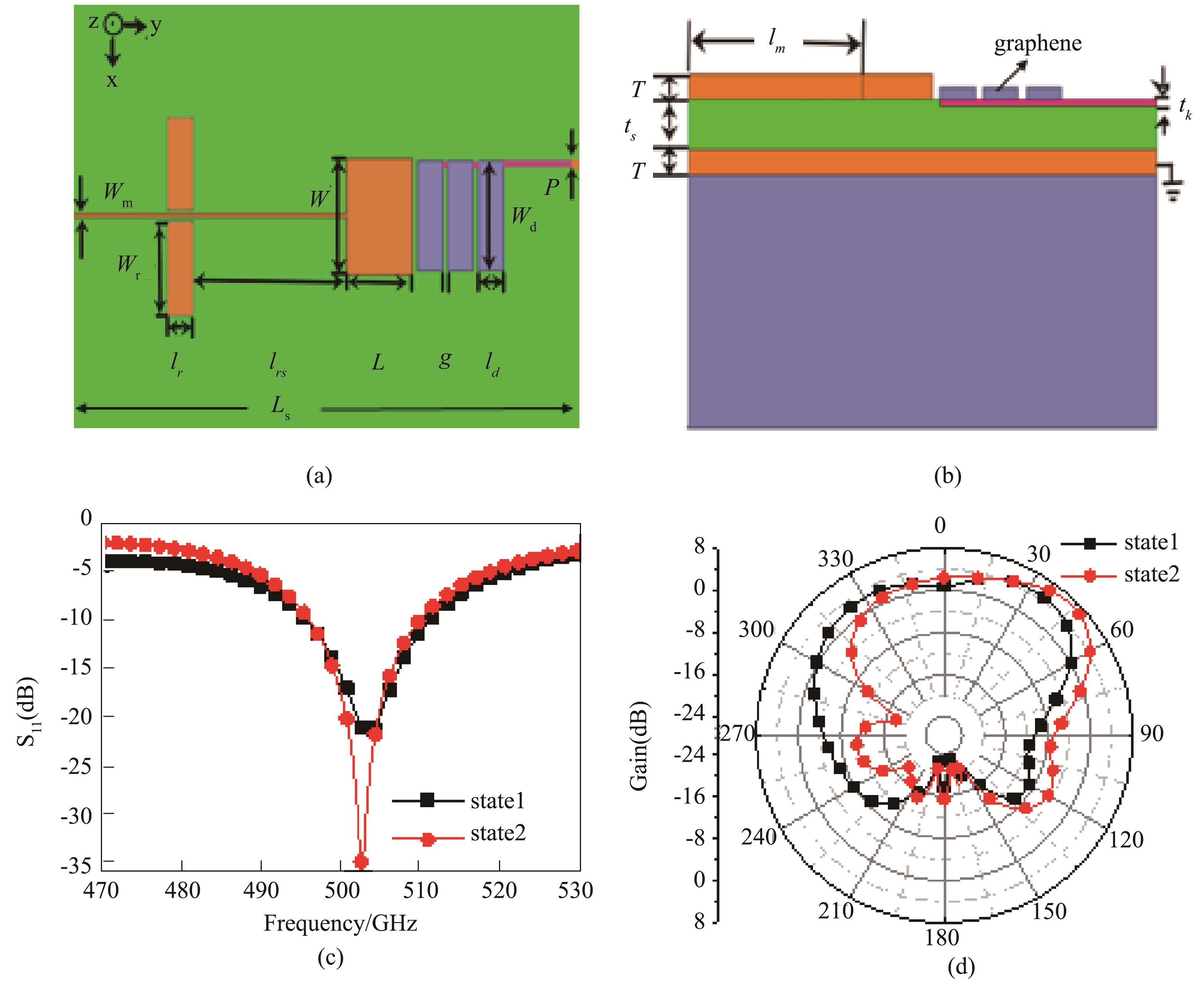
Figure 1.Schematic of the proposed antenna and the basic performance parameters, (a) Top view, (b) Side view, (c) Reflection coefficient S11, and (d) Simulated radiation patterns in E-plane for the two working states of the antenna (states 1 and 2 for the cases of unbiased and biased)
The features of the proposed antenna are numerically simulated with the ANSYS High Frequency Structure Simulator (HFSS) software [33]. The antenna working at 500 GHz and operating frequency range of the antenna is from 470 GHz to 530 GHz. The wave port excitation mode is selected and the input impendence is set to 50 Ω. The layered impedance boundary condition is used for the thin graphene patches. Each graphene patch has two states. If a high bias voltage (Fermi energy µc=1 eV, denoted as “1”) is applied to the graphene patches, the conductivity of the graphene patches will significantly increase. This will result in the metal-like behavior of graphene patches, and the graphene patches work as directors as in the conventional Yagi-Uda antenna. On the contrary, once a low or no bias voltage (Fermi energy µc=0 eV, denoted as “0”) is applied to the graphene patches, they will behave as thin dielectric layers, which have no essential influence on the behavior of the patch antenna. Depending on the different bias voltages applied to the graphene patches, the antenna can work in two different states (state 1 for µc=0 eV and state 2 for µc=1eV).
Fig. 1(a) and (b) show the schematic of the antenna. The substrate is a high resistivity silicon wafer with the size of Ls× Ls and Ls=1.8 mm the length and width. There is a copper ground layer with thickness T on the high resistivity silicon substrate. A 30-μm-thick (ts) SiO2 dielectric cavity layer is on the metallic ground layer. The relative permittivity of SiO2 is εr =4. The size of the micro-strip fed line is lm×wm, the driven patch is L×W, and the thickness of both of the micro-strip fed line and the driven patch is T. The size of the reflector patches is lr×wr, the distance between the reflector patch and the driven patch is given by lrs. The graphene patches are used as the director in the Yagi-Uda antenna, the size of which is given by ld×wd, and the gap between the two graphene patches is given by g. The p-doped silicon strips beneath the graphene patches are used as electrical connections between the metallic gating pads and the graphene patches, and the thickness of the doped Si strip is given by tk. The dimension of the driven copper patch is p×p. As reported in Ref. [34], We can calculate the theoretical value of the length (L) and width (W) of the driven patch. Further, L, W and other parameters of the antenna are optimized by simulation and the results are listed in Table 1.
| L | 130 | wm | 5 | lrs | 300 | g | 8 |
|---|
| W | 190 | lr | 50 | ld | 50 | T | 0.2 |
| lm | 540 | wr | 150 | wd | 179 | ts | 30 |
| tk | 0.2 | p | 10 | | | | |
Table 1. Antenna parameters (units: µm)
Fig. 1(c) depicts the reflection coefficients S11 for the antenna working in state 1 and state 2 for the proposed antenna. The antenna is resonating at 500 GHz, and the -10 dB return loss bandwidth is about 3% (495 GHz - 510 GHz). When the antenna is in state 1 and state 2 respectively, the simulated radiation pattern in E-plane (where the electric field vector and the maximum radiation direction are located) of the proposed antenna is shown in Fig. 1(d). It can be observed that in E-plane when the antenna is in state 1, the antenna behaves as a conventional patch antenna. When the antenna is in state 2, the angle of the main lobe veers round to along the graphene patches. This confirms the effect of the graphene director on the radiation direction of the antenna.
2.2 QYU antenna with two groups of directors
The antenna structure shown in Fig. 1 confirms the guiding effect of the graphene director on the beam direction in E-plane. But it cannot achieve the beam shift in thezenith angle direction. To overcome this deficiency, we design an improved antenna structure shown in Fig. 2(a). Compared with the former antenna structure, the graphene-patch director is divided into two groups, and each of the two groups is similar to the director in the conventional Yagi-Uda antenna. The gap between the graphene patches along the y-axis is g=8 µm and the widths of all the gaps are the same. All the graphene patches have the same size, given by ld2=129 µm and wd2=94 µm. To realize strong coupling between the driven patches and the two neighboring graphene patches of the director, a very small value of s=0.5 µm is chosen. In order to keep strong couplings between the neighboring graphene patches within the same group, the parameters ld2 and g are optimized, and the parameters h1=39 µm and h2=76 µm are also optimized to realize a higher gain. The two groups of graphene directors are labeled as D1 and D2, respectively. Depending on the different bias voltages applied to the graphene patches, the antenna can work in three different states, (state 1: (1,0) with µc=1 eV for graphene patches in D1 and µc=0 eV for graphene patches in D2; state 2: (0,1); and state 3: (1,1)).
Figure 2.(a) Schematic of the antenna with two groups of directors, (b)Reflection coefficient S11, (c) E-plane radiation pattern and (d) θ=60° plane radiation pattern of the proposed antenna operating at different states.
Fig. 2(b) shows the reflection coefficient S11 of the proposed antenna. The resonant frequency of the antenna is about 500 GHz, and for different working states of the antenna, the resonant frequency reveals a tiny shift. It is because that the effective impedance of the graphene directors and the driven patch is a little different when the antenna works in different states. The -10 dB return loss bandwidth is about 2.5%.
Fig. 2(d) shows the radiation pattern of the antenna in θ=60° plane. It can be observed that, when the antenna is in states 1, 2, and 3, the angles of the main lobe in θ=60° plane are about 120°, 60°, and 90°, respectively. Thus, the angle of the main lobe for the antenna in θ=60° plane can be swept from 60° to 120°. While in the E-plane, the angle of the main lobe is fixed at about θ=60°, as shown in Fig. 2(c).
2.3 QYU antenna with three groups of directors
For the antenna structure mentioned in subsection 2.2, the main lobe can be swept from 60° to 120° in θ=60° plane. In order to increase the steering angle, a QYU antenna with three groups of graphene-patch directors is considered. In this case, we find that a rectangle driven metallic patch does not work well. Therefore, the driven metallic patch is changed from a rectangle patch to a half-round patch, and the structure of the improved antenna is shown in Fig. 3(a).
Figure 3.(a) Structure of the antenna with three groups of directors, (b) Reflection coefficient S11 of the proposed antenna operating at different states, (c) E-plane radiation pattern, and (d) Radiation pattern in θ=60° plane
Fig. 3(a) shows the structure of the antenna with three groups of graphene-patch directors. Different from the former two antennas, the driven patch is a half-round patch. The graphene patches are divided into three groups, and each of them is similar to the director in the conventional Yagi-Uda antenna. The diameter of the driven patch is W1=370 µm, and the distance between the reflector patch and the driven patch is lrs=175 µm. The gap between two neighboring graphene patches in the first and the third group is given by g1=15 µm, and the gap between two neighboring graphene patches in the second group is given by g=20 µm. The angle of graphene patches in each group is given by α1=58°, α2=40.3°, and α3=30.2° respectively, and the width of the graphene patch is given by ld3=100 µm. The three groups of graphene directors are labeled as D1, D2, and D3,respectively. Depending on the different bias voltages applied to the graphene patches, the antenna can work in six different states, (state 1: (1,0,0) with µc=1 eV for graphene patches in D1 and µc=0 eV for graphene patches in D2 and D3; state 2: (1,1,0); state 3: (0,1,0); state 4: (0,1,1); state 5: (0,0,1) and state 6: (1,1,1)).
Fig.3(b) shows the simulated reflection coefficient S11 of the antenna. The resonant frequency of this antenna is around 500 GHz. In all working states, good impedance matching with the return loss S11<-30 dB is obtained around the resonant frequency. The -10 dB return loss bandwidth is about 8%.
Fig. 3(d) shows radiation patterns of the proposed antenna in the θ=60° plane operated at different states. One can see that in state 1, only D1 works as a director, and the angle of the main lobe is 150°. In state 2, both D1 and D2 work as directors, and the angle of the main lobe is 110°. In state 3 only D2 works as a director, and the angle of the main lobe is 90°. Because of the symmetry of the antenna, the radiation patterns of the antenna working in states 4 and 5 and working in states 1 and 2 will be symmetric about the y-axis. Thereby the beam in θ=60° plane of the antenna can be deflected from 30° to 150°. While the angle of the main lobe in E-plane is fixed at about θ=60°, as shown in Fig. 3(c). The maximal values of gain are in the range of 6.5 dB - 8.7 dB. The angles of the main lobe and the maximal values of gain for the antenna in different working conditions are shown in table 2.
| Working state of antenna | 1 | 2 | 3 | 4 | 5 | 6 |
|---|
| Return loss (dB) | -36 | -32 | -43 | -32 | -36 | -44 |
| Voltage standing wave ratio (VSWR) | 1.03 | 1.12 | 1.01 | 1.12 | 1.03 | 1.01 |
| -10 dB bandwidth | 9% | 12% | 8% | 12% | 8% | 14% |
| Angle of main lobe (φ) | 150° | 110° | 90° | 60° | 30° | 90° |
| Gain (dB) | 6.6 | 7.8 | 8.7 | 7.8 | 6.6 | 7.5 |
| Radiation efficiency | 85% | 90% | 85% | 90% | 85% | 96% |
Table 2. Antenna performance
Fig. 4(a-1)-(a-4) and (b-1)-(b-4) show the 3D radiation patterns that are observed from different perspectives of the antenna. From the 3D radiation patterns, the beam reconfigurable ability can be seen clearly. Fig. 4(c-1)-(c-4) show the surface current distributions for the proposed antenna in different working conditions. It is easy to see that different group graphene patches of the antenna are resonating in different working conditions. For instance, in state 1, as shown in Fig. 4(c-1), only D1 is resonating, the surface current is excited only on D1 and it works as a director, the other graphene patches with µc=0 eV have no effects on the behaviors of the antenna. While in state 2, only D1 and D2 are resonating. Because of the symmetry of the structure, the surface current distributions of the antenna working in states 4 and 5 and the antenna working in states 2 and 1 will be symmetric about the y-axis. The variations of radiation patterns are well-explained by the current distributions of the antenna working in different states. And the capacitive structure is used to apply bias voltages to graphene patches to achieve electrical regulation. Therefore, when a bias voltage is applied to graphene, there is no current distribution or voltage drop on the surface, and the voltage is evenly distributed.
Figure 4.(a-1)~(a-4) and (b-1)~(b-4), 3D radiation patterns in different planes.(c-1)~(c-4) Surface current (Js) distributions for the proposed antenna in different working states. (a-1), (b-1), and (c-1) for state 1; (a-2), (b-2), and (c-2) for state 2; (a-3), (b-3), and (c-3) for state 3; (a-4), (b-4), and (c-4) for state 6.
3 Discussion
In this Section, the effects of the relaxation time in graphene and the p-doped silicon strip are discussed. The graphene quality is primarily determined by the relaxation time. In the above simulations, the relaxation time 20 ps in graphene is selected. In Fig. 5(a), several relaxation times in the range of 0.1-20 ps are set in the simulations. The numerical results show that the relaxation time has a negligible effect on the angle of the main lobe and very little effect on the gain of the antenna. The gain of the antenna increases with the increase in relaxation time.
Figure 5.(a) and (b) Radiation patterns of antenna proposed in Section 2.2, (a) With different electron relaxation times in graphene, (b) With and without p-doped silicon strips,(c) and (d) Radiation patterns of antenna proposed in section 2.1, (c) With different bias voltages applied to the graphene-patch directors, and (d) With graphene-patch directors with µc=0 eV and without graphene-patch directors.
We also study the effects of the p-doped silicon strips. As shown in Fig. 5(b), the p-doped silicon strips have negligible effects on antenna performance. The electron plasma frequency is [35]
where n0 is the electron density, e is the electron charge, me is the electron effective mass, ε0 is the vacuum dielectric constant and ε is the dielectric permittivity.
The p-doped silicon, which we choose has a very low doping concentration (1e15 cm-3), from equation (5), the electron plasma frequency of the p-doped silicon is 116 GHz, which is much less than the antenna working frequency (500GHz). Thus, the p-doped silicon trips have negligible effects on antenna performance.
The magnitudes of bias voltages applied to the graphene patches are considered for the antenna mentioned in section 2.1, as shown in Fig. 5(c). As the Fermi energy increase from µc=0 eV to µc=1 eV, the graphene patches change from dielectric layers to mental-like layers, and the angle of the main lobe in E-plane converts from θ=0° to θ=50°. Especially when the Fermi energy is lower than 0.4 eV, the graphene patches cannot be operated as directors, and when the Fermi energy is higher than 0.5 eV, the graphene patches gradually behave as metal-like layers and work as directors. Furthermore, if the Fermi energy µc=0 eV, as shown in Fig. 5(d), the radiation patterns of the antenna are almost the same as those of the antenna without graphene patches. This indicates that the graphene patches with µc=0 eV mainly behave as dielectric layers.
4 Conclusion
In this work, reconfigurable QYU micro-strip antennas with graphene-patch directors are proposed. Because the complex conductivity of graphene can be tuned by changing the bias voltages, the graphene patches can be electrically switched between metallic state and dielectric state. Therefore, the graphene-patch directors can be electrically reconfigurable and the main lobe angle of the antenna can be electrically swept in a large range in θ=60° plane (60° to 120° for the configuration of two graphene-patch directors and 30° to 150° for the configuration of three graphene-patch directors). The reconfigurable behaviors of the antenna are not sensitive to the scattering time of graphene. It is expected that such a graphene-based antenna is attractive for THz application in the future.
References
[1] J Costantine, Y Tawk, S E Barbin. Reconfigurable antennas: Design and applications, 103, 424-437(2015).
[2] B Z Wang, S. Xiao, Y. Bai. Researches on pattern reconfigurable antenna and its application in phased array. 2011,, 46-49.
[3] C G Christodoulou, Y Tawk, S A Lane. Reconfigurable antennas for wireless and space applications. Proc. IEEE, 100, 2250-2261(2012).
[4] Geim A K and Novoselov K S, The rise of graphene. Nature Mat,, 6, 11-19(2009).
[5] Geim A K, Graphene: Status and prospects. Science, 324, 1530-1534(2009).
[6] J B Li, H X Liu, L Wu. The photoelectric property of graphene modified by boron and nitrogen atoms from density functional theory calculation. J. Infrared Millim. Waves, 37, 25-29(2018).
[7] Q Zhang, L B Tang, R J Li. Graphene oxide: progress in preparation, reduction and application. J. Infrared Millim. Waves, 38, 79-90(2019).
[8] M Dragoman, A A Muller, D Dragoman. Terahertz antenna based on graphene. Journal of Applied Physics, 107, 104313(2010).
[9] I Llatser, C Kremers, D N Chigrin. Characterization of graphene-based nano-antennas in the terahertz band, 194-198(2012).
[10] Y Huang, L S Wu, M Tang. Design of a beam reconfigurable THz antenna with graphene-based switchable high-impedance surface. IEEE Transactions on Nanotechnology, 11, 836-842(2012).
[11] Z Xu, X D Dong, J Bornemann. Design of a reconfigurable MIMO system for THz communications based on graphene antennas, 4, 609-617(2014).
[12] Y L Wu, M J Qu, L X Jiao. Graphene-based Yagi-Uda antenna with reconfigurable radiation patterns. AIP Advances, 6, 065308(2016).
[13] Yagi H, Beam transmission of the ultra-short waves. Proc. IRE, 85, 1864-1874(1997).
[14] S Zhang, G H Huff, J Feng. A pattern reconfigurable micro-strip parasitic array. IEEE Trans. Antennas Propagat, 52, 2773-2776(2004).
[15] H Lim S and Ling. Electron. Lett, 43, 1326-1327(2007).
[16] X S Yang, B Z Wang, W Wu. Yagi patch antenna with dual-band and pattern reconfigurable characteristics. IEEE Antennas Wireless Propag. Lett, 6, 168-171(2007).
[17] X S Yang, B Z. Wang, Y Zhang. Microw. Opt. Technol. Lett, 42, 296-297(2004).
[18] Huang J and Densmore A C, Micro-strip Yagi array antenna for mobile satellite vehicle application. IEEE Trans. Antennas Propagat, 39, 1024-1030(1991).
[19] K Novoselov, A K Geim, S V Morozov. Electric field effect in atomically thin carbon films. Science, 306, 666-669(2004).
[20] K S Novoselov, S V Morozov, T Mohiuddin. Electronic properties of graphene. Physica Status Solidi (b), 244, 4106-4111(2007).
[21] L Maeng, S Lim, S J Chae. Gate-controlled nonlinear conductivity of Dirac fermion in graphene field-effect transistors measured by terahertz time-domain spectroscopy. Nano Letters, 12, 551-555(2012).
[22] M Dawlaty, S Shivaraman, J Strait. Measurement of the optical absorption spectra of epitaxial graphene from terahertz to visible. Applied Physics Letters, 93, 131905(2008).
[23] V P Gusynin, S G Sharapov, J P Carbotte. Magneto-optical conductivity in graphene. Journal of Physics: Condensed Matter, 19, 026222(2007).
[24] J Horng, C F Chen, B Geng. Drude conductivity of Dirac fermions in graphene. Physical Review B, 83, 165113(2010).
[25] W Liu, R V Aguilar, Y F Hao. Broadband microwave and time-domain terahertz spectroscopy of chemical vapor deposition grown graphene. Journal of Applied Physics, 110, 083510(2011).
[26] J L Tomaino, A D Jameson, J W Kevek. Terahertz imaging and spectroscopy of large-area single-layer graphene. Optics Express, 19, 141-146(2011).
[27] L Ren, Q Zhang, J Yao. Terahertz and infrared spectroscopy of gated large-area graphene. Nano Letters, 12, 3711-3715(2012).
[28] N Rouhi, S Capdevila, D Jain. Terahertz graphene optics. Nano Research, 5, 667-678(2012).
[29] B Sensate, R Yan, M M Kelly. 1038. ” Nature Communications, 3, 10(2012).
[30] K S Novoselov, A K Geim, S V Morozov. Two-dimensional gas of massless Dirac fermions in graphene. Nature, 438, 197-200(2005).
[31] J Costantine, Y Tawk, S E Barbin. Reconfigurable antennas: design and applications, 103, 424-437(2015).
[32] F Liang, Z Z Yang, Y X Xie. Beam-scanning microstrip quasi-YagiUda-antenna based on hybrid metal-graphene materials. IEEE Photonics Technology Letters, 12, 1127-1130(2018).
[33] Ansoft HFSS. [online](15).
[34] A B Constantine. Antenna theory: analysis design, third edition. Inc, 811-882(2005).
[35] J S Blakemore. Semiconducting and other major properties of gallium arsenide. Journal of Applied Physics, 53, 101063(1981).