
Navid Bani Hassan, Fahimeh Dehkhoda, Enyuan Xie, Johannes Herrnsdorf, Michael J. Strain, Robert Henderson, Martin D. Dawson, "Ultrahigh frame rate digital light projector using chip-scale LED-on-CMOS technology," Photonics Res. 10, 2434 (2022)
- Photonics Research
- Vol. 10, Issue 10, 2434 (2022)
Abstract
1. INTRODUCTION
Digital light projection (DLP) systems are now a well-established technology, with advances driven by the demands of cinematic and consumer markets. Systems with kiloframes per second (kfps) update rates and pixel counts in the megapixel range are widely available, serving both consumer video and scientific applications. Commercial developments are strongly driven by demand for high pixel count devices for digital projection and displays, though a number of other application areas have emerged including optical wireless communications [1], data through display [2–5], visible light positioning [6], single-pixel and 3D imaging [7–13], optomechanical manipulation [14], fluorescence lifetime imaging [15], and optogenetic stimulation [16,17]. These applications benefit from, or even require, pixel modulation rates well beyond the typical frame rates of visual displays.
Current commercially available DLP systems are mainly based on two forms of non-self-emissive technology, liquid crystal displays (LCDs) and digital micromirror displays (DMDs) [18,19]. LCDs use electronic control of nematic liquids, commonly sandwiched between polarization films, to control the absorption or phase change of light through a pixel [19]. DMDs are based on microelectromechanical systems (MEMS) devices, where the reflective surface of a pixel can be orientated to pass or block incident light through the projection path [18]. DMDs are particularly attractive due to their pixel switching times and compatibility with drive electronics. While commercial development has enabled the impressive resolution of these systems, their frame rate is limited by the physical motion required to switch pixels and the data-handling capacity required to update megapixels frames. Furthermore, gray-scale operation of DMD displays uses duty-cycle control of pixel switching [18], consequently reducing the maximum achievable frame rate of the device inversely with the number of gray levels required.
In parallel to these developments, advances in semiconductor materials, and in particular the III-nitrides, have enabled the realization of high brightness LED pixel emitters with dimensions from the millimeter to micrometer range [20]. The spectral quality, high brightness, and potential for integration with electronic backplanes, have seen deployment of these devices in displays ranging in dimension from mobile phone interfaces to super-large screen installations for advertising or theatrical installations. In addition to their emissive properties, LED pixels have another key advantage to offer in DLP systems: namely, their high modulation bandwidth, with individual devices demonstrated at up to gigahertz rates [21], and the potential for short pulse emission in the subnanosecond regime [22].
Sign up for Photonics Research TOC. Get the latest issue of Photonics Research delivered right to you!Sign up now
The planar format of LED pixel arrays allows them to be directly interfaced with electronic drive chips, for example, through flip-chip bonding [23]. Arrays of LEDs with individual pixel control electronics represent a new form of compact microdisplay/projector [20]. In previous work, we have reported on LED arrays with
In this work, we present a custom-designed chip-scale LED-on-CMOS DLP using a
This paper presents the performance of the chip in each operation mode, in addition to an example application in high-speed optical camera communications (OCCs), where we demonstrate
2. DLP HARDWARE
The device presented here is an array of
A. Device Fabrication
The LED array was fabricated using a c-plane GaN-on-sapphire wafer with standard LED fabrication processes that follow the design guidelines in Ref. [25]. Figure 1 shows microscope images of the fabricated CMOS driver chip and LED array system.
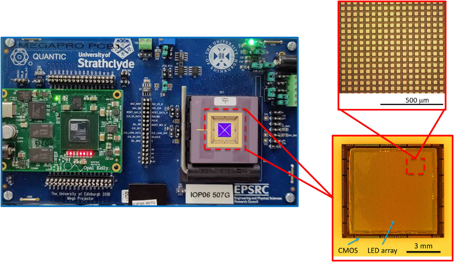
Figure 1.Photograph of the mounted LED projector on CMOS chip, co-packaged with an FPGA controller. The projector is here displaying a diagonal cross pattern. Magnified inset images show the mounted LED array on the CMOS chip and a zoomed view of the LED pixel contact pads, imaged through the sapphire substrate.
The initial prototypes reported here emit at 450 nm, though the entire wavelength range of the GaN material system (
B. Smart Pixel Driver Details and Functionality
Each individual pixel driver on the chip comprises a 5-bit current digital-to-analog converter (DAC), a separate current source with 2 mA driving capability, a 2-bit in-pixel memory for high-speed pattern toggling, and control signals to enable different operation modes. Figure 2 shows a schematic circuit diagram of these elements and their connections. The chip infrastructure that supplies signals and power to each pixel is detailed in Appendix B. A simplified timing diagram is presented in Fig. 3.
![]()
Figure 2.Simplified schematic of the driver circuit for one pixel, showing 5-bit DAC, in-pixel memory, and control signals.
![]()
Figure 3.Simplified timing diagram of the digital control signals supplied to the CMOS by an FPGA.
The optical output power of a single pixel driven by the DAC is shown in Fig. 4(a), and a good linear behavior is observed in the output power apart from a small kink between gray levels 15 and 16, which is a well-known effect in this type of CMOS current DAC [30]. An example of a gray-scale image [the project logo of the Engineering and Physical Sciences Research Council (EPSRC)-supported QuantIC program; see Funding and Acknowledgement sections] from the device is shown in Fig. 4(b). If a sequence of binary patterns is being displayed, the DAC can be used to either superimpose a gray-scale image or mitigate possible manufacturing variations in pixel brightness. It is also possible to display a sequence of true gray-scale patterns at up to 83 kfps, in which case predistortion or postequalization techniques can be used to mitigate pixel brightness variations.
![]()
Figure 4.(a) Optical output power of a single pixel for different DAC settings; (b) gray-scale image from the LED projector chip using the DAC gray levels; (c) digital version of the image projected in (b).
3. DEMONSTRATION OF SYSTEM OPERATION MODES
There are four different modes of pattern switching accessible using the custom driver chip:
Mode 1 can be accessed for both binary and gray-scale pattern projection. Modes 2 and 3 are accessible for binary patterns. In all cases, gray-scale information can be prestored on-chip and the binary pattern projection, toggling or pulsing, can be applied on top of this pre-existing bias set point. Details of each operation mode are presented in the following sections.
A. High-Speed Pattern Projection and OCC
For binary pixel on–off state information, there are two update modes: rolling and global pixel update. For these cases, a single, full-frame, binary pattern can be loaded onto the chip within 2 μs, thus enabling 0.5 Mfps at full resolution. In the rolling pixel mode, each pixel is updated individually in sequence, with the value held until the next update. In the global pixel mode, the full frame is refreshed in one shot once all of the pattern data are loaded.
In addition to the binary pixel on–off data, gray-scale values can be sent to each pixel in the array. Significantly, in contrast to DMD devices, the gray-scale value corresponds to the pixel drive current and is not a duty cycle effect that relies on multiple binary frames for implementation. The gray-scale pattern that is held by the 5-bit in-pixel DAC can be loaded within 12 μs, corresponding to 83 kfps. As detailed in Appendix B, input data can be selectively written to the binary pixel state or the DAC, corresponding to the switch control signal. Therefore, a gray-scale image can be stored on the chip and used as a set point for rapid pixel on–off modulation.
To demonstrate the potential of this high-speed binary projection, we used it in an OCC application. Full details of the experimental setup and data handling are presented in Appendix C. The camera was sampling at 0.8 Mfps, and the projector operated at 0.25 and 0.4 Mfps, the latter corresponding to the camera’s Nyquist sampling limit. Figure 5 shows eye diagrams and detected symbol level histograms for
![]()
Figure 5.(a) Measured eye diagram for
The eye diagram for the 0.25 Mfps case is very clear and represents error-free transmission (for the
B. High-Speed Pattern Toggling
Using the 2-bit in-pixel memory function, it is possible to exceed the switching rate of the data projection modes detailed above in a two-pattern toggling mode. In this mode, two independent frames can be stored using the in-pixel memory and switched using a global clock signal. Toggling was first assessed using the same setup as for OCC. We selected two pattern sets for the projector system toggling tests: (1) checkerboard switching to all pixels off (C2B) and (2) two spatially complementary checkerboard (C2C) patterns. Figure 6 shows raw captured images, where each image shows a
![]()
Figure 6.Representative LED projection frames captured with a high-speed camera at 0.8 Mfps. Visible is the partial footprint of the last two columns of the LED chip: (a) frame #1 C2B, (b) frame #2 C2B, (c) frame #1 C2C, and (d) frame #2 C2C. (e) Measured photosignal from global array toggling at 2 Mfps.
To determine the pattern switching limits, the array was toggled between all pixels off and a pattern with all pixels on at the highest DAC setting of 31, and the optical output was measured with a photomultiplier tube (PMT). Figure 6(e) shows the recorded waveform at a toggling rate of 2 Mfps. Above 2 Mfps, a reduction in duty cycle and peak power was observed, and at 8 Mfps, the duty cycle had reduced to 25%. This behavior was independent of the number of pixels that were switched.
C. Nanosecond Pulsed Mode
Compared with other display technologies, the micro-LED platform has the unique capability of directly emitting nanosecond optical pulses [22]. In the device presented here, this capability is accessed through the 2-mA driver, which is controlled by a separate global control signal that can be switched on a nanosecond time scale. Pixels are enabled to respond to the global pulse signal superimposed with the binary pattern, thus allowing spatial patterns to be pulsed, where the patterns can be updated at the same rate, as detailed previously. The nanosecond pulsing function was assessed by loading binary patterns with different numbers and distributions of active pixels, and pulsing them with electronic pulse widths between 5 and 100 ns at repetition rates between 10 and 100 MHz. The optical pulses were resolved using a PMT connected to an oscilloscope with 1 GHz bandwidth, and the spatial patterns were verified using a slow-response optical camera.
Figure 7(a) shows a representative spatial projection pattern that is being driven in nanosecond pulsed mode. Representative temporal waveforms at 10 MHz repetition rate, 5 ns pulse duration, and with the number of active pixels as a parameter, are shown in Fig. 7(b), highlighting the consistent pulse shape over a wide range of active device numbers. The number of active pixels is limited to
![]()
Figure 7.(a) Optical micrograph of a pattern displayed in nanosecond pulsed mode; (b) optical waveform of 5 ns long pulses as a function of number of pulsing pixels; (c) optical pulse duration as a function of the number of pixels for a 5 ns input pulse; (d) optical pulse duration as a function of electrical input pulse duration; (e) relative delay of the pulses emitted by individual pixels within one row; (f) relative delay of the pulses emitted by individual pixels within one column.
To assess the effect of the distribution of the global pulse signal in the nanosecond time regime, the timing delay of emitted pulses across the array was measured. Local arrays of the LED chip were imaged onto the PMT, and the received signal was compared to the pulse trigger signal to measure relative delay. Figures 7(e) and 7(f) show the relative time delay between optical pulses emitted by individual pixels at various locations on the chip, arranged by column or row, respectively. The time delay between columns on-chip does not show a clear trend, with a scatter of
The emitted optical pulse energy depends on the number of active pixels, as shown in Fig. 8, where the pulse duration was 5 ns and the repetition rate was 10 MHz. From Fig. 8(a), the total aggregated pulse energy increases as a function of active pixel number, then goes through a turning point, reducing as further pixels are added, beyond
![]()
Figure 8.(a) Total chip pulse energy for 5 ns-long pulses as a function of the number of active pixels at 10 MHz, and (b) pulse energy per pixel as a function of number of active pixels.
4. DISCUSSION
The LED-on-CMOS-based DLP system demonstrates absolute frame rates in both binary and true gray scale that exceed what is possible with current DMD- or LCD-based systems, and can be modulated with pulse times down to the nanosecond range. In addition, the single chip-scale emissive display does not require the external light source and optics necessary for transmissive or reflective DLPs, making it a compact optoelectronic component, easily integrated with printed circuit board (PCB) packaging. It is worth setting its performance in context with the current state of the art, particularly in DMD-based systems, with respect to the envisaged application areas.
The absolute frame rate of a DLP system is a crucial feature in scientific imaging applications, including spatially patterned computational imaging schemes [9–11,13], or where multiple functions can be realized simultaneously, for example, transmission of high-speed data on top of lower rate positioning or imaging illumination [6]. For example, a compression-free single-pixel camera with
![]()
Figure 9.Comparison of the LED array presented here with other 2D programmable pattern sources, with pixel count and frame rate as parameters. Note the scaling potential of our technology in terms of number of pixels. Details of individual devices are provided in
The absolute frame rate of our system for a binary pattern projection is 0.5 Mfps, compared with a few tens of kiloframes per second for DMD-based systems (e.g., 60 kfps for the BMC Hex 1011). For two-pattern toggling, our system rate increases to
In this work, we demonstrated pulsed pixel operation of 4 ns minimum duration at a repetition rate of 100 MHz, and previous LED devices have shown subnanosecond capability [22]. These time scales are compatible with time-correlated single-photon counting (TCSPC) applied, for example, to fluorescence lifetime imaging or time-of-flight ranging [8,15]. Crucially, this function is overlaid with the binary pattern projection, which allows content adaptive illumination for TCSPC and/or a combination of TCSPC with electro-optical trapping [14]. In order to combine such short pulse performance with spatiotemporal patterning, one would otherwise have to combine a lower frame-rate transmissive or reflective spatial light modulator with a pulsed laser, thus increasing complexity, footprint, and cost of the system.
The form factor of the DLP system can also be an important factor in systems design, and the emissive nature of the device presented here presents a contrast with traditional DLP technology. The use of external light sources with modulator type DLPs allows them to employ a wide variety of sources to fit application needs, including broadband LEDs, single-frequency laser sources, or ultrashort pulsed lasers. The trade-off in this arrangement is the space requirement for external coupling optics and the sources themselves, which need to be packaged together. In contrast, the LED-based DLP can be mounted on flat-panel electronic circuit boards with only output coupling optics required. The DLP system presented here makes use of LED emitters for their high brightness, direct electronic emission control, and potential for high bandwidth modulation. The device here consumed 5 W of electrical power during the experiments shown above, which compares to a value of 10 W for a typical commercial DMD (Texas Instruments DLP9000), not including the power requirements of the external light source required.
While the capabilities of the chip have been discussed here in the main as a source for imaging and sensing applications, it should be noted that they also present significant potential as high-speed pattern-programmable excitation sources for a wide range of experimental and engineering systems. The low size weight and power consumption metrics of the device make it particularly attractive for low-cost deployment where concurrent data communications and positioning or imaging functions are required, for example, in light-fidelity (LiFi) settings or for autonomous vehicle systems. Finally, the high-speed, highly parallel optical pattern generation could be used as a multiplexed optical pump source for physical effects including quantum-dot-based single-photon emission, nanowire photonics on-chip or spatial light modulators based on fast optical absorption modulation effects. In future, LED wavelengths from the UV to the NIR could be employed to access applications including high-speed, mask-free photolithography, or scene-adaptive IR time of flight imaging.
5. CONCLUSION
By employing micro-LED emitters as elements in DLP systems, a number of complementary modes of operation can be achieved, with frame update rates significantly higher than current mechanically based systems, while having lower size weight and power requirements. We have presented a smart pixel control CMOS drive chip directly bonded to an emissive micro-LED pixel chip with an active pixel count
Acknowledgment
Acknowledgment. We thank Fraunhofer IZM for their help with flip-chip bonding. The authors thank Graeme Johnstone for help with the toggle mode characterization.
APPENDIX A: DETAILED DESIGN SPECIFICATIONS AND PERFORMANCE PARAMETERS
Table
Design Specifications and Performance Parameters
| Parameter | Value | Additional Detail |
|---|---|---|
| Array dimensions | ||
| Pixel pitch | 50 μm | |
| Pixel active area | ||
| Pixel fill factor | 36% | Light-emitting area |
| Frame rate | 0.5 Mfps | Limited by 8 Gb/s digital electronic interface between external FPGA controller and LED chip |
| Frame update mode | Global/rolling | Both available irrespective of frame rate |
| Pattern toggling rate | 2 MHz | 8 MHz possible at compromised duty cycle/intensity |
| Rise time | 315 ns | All pixels off to all pixels on |
| Fall time | 8 ns | All pixels on to all pixels off |
| Frame rate (gray scale) | 83 kfps | Limited by 8 Gb/s digital electronic interface between external FPGA controller and LED chip |
| Number of gray values | 32 | 5 bit |
| LED current | 87 μA | Single pixel; highest gray level setting |
| Optical output power | 22 μW | Single pixel; highest gray level setting |
| Display brightness | LEDs emitting at 450 nm wavelength | |
| Maximum pulse repetition rate | 100 MHz | |
| Minimum pulse duration | 4 ns | Limited by external controller |
| Pulse energy | 0.08 pJ | Single pixel at 4 ns, 20 μW peak power |
| 17 pJ | Pattern with 1000 active pixels at 4 ns, 1.5 A peak current |
The LED array was flip-chip bonded onto the CMOS driver chip using an indium-based bonding process, and the flip-chip bonded device was packaged and wire-bonded into a ceramic package, which can be inserted into a socket on a custom-made printed circuit board. The digital control signals to the CMOS chip are supplied by an Opal Kelly XEM7310-A200 field-programmable gate array (FPGA). A total of six LED chips were fabricated for this work, all of which emit at 450 nm. In principle, any wavelength supported by the GaN material system can be used, i.e.,
The DAC was designed to provide currents ranging from 0 μA (gray level 0) to 87 μA (gray level 31). The current levels per pixel were chosen in order to reduce electrical cross talk and to keep the maximum current across the entire chip on the order of 1 A, which is a value that was found to be sustainable by previous generations of CMOS-controlled micro-LED arrays [
APPENDIX B: CMOS SMART PIXEL DESIGN
The detailed block diagram of the CMOS chip is provided in Fig.
![]()
Figure 10.Schematic diagram of the signal distribution circuit of the CMOS driver chip.
![]()
Figure 11.Detailed timing diagram of gray-scale and binary-pattern loading.
Figure
Figure
APPENDIX C: HIGH-RATE PATTERN PROJECTION EXPERIMENTS
In order to demonstrate that a frame rate of 0.5 Mfps for binary patterns and 83 kfps for gray-scale patterns are indeed achieved, the signal “LOAD_CLK” was monitored while loading a single pattern. The signal “LOAD_CLK” is a digital signal that alternates between logic high and low for the entire duration of the pattern load process and is continuously logic low while no pattern is loaded. Figure
![]()
Figure 12.Oscilloscope traces of the signal “LOAD_CLK” in Fig.
![]()
Figure 13.Statistics from the camera communications experiment. (a) Histogram of time-average pixel intensity, (b) BER at 0.25 Mfps versus time-averaged pixel intensity, and histograms of BER at (c) 0.25 Mfps and (d) 0.4 Mfps.
Figure
References
[10] T. Weise, B. Leibe, L. V. Gool. Fast 3D scanning with automatic motion compensation. IEEE Conference on Computer Vision and Pattern Recognition, 1-8(2007).
[19] H. Kawamoto. The history of liquid-crystal displays. Proc. IEEE, 90, 460-500(2002).
[24] J. Herrnsdorf, J. J. D. McKendry, E. Xie, M. J. Strain, I. M. Watson, E. Gu, M. D. Dawson. High speed spatial encoding enabled by CMOS-controlled micro-LED arrays. IEEE Photonics Society Summer Topical Meeting Series (SUM), 173-174(2016).


Set citation alerts for the article
Please enter your email address

© Copyright 2018-2021 | Chinese Laser Press. All Rights Reserved 沪ICP备15018463号-20