• Journal of Semiconductors
  • Vol. 45, Issue 3, 032401 (2024)
Zhenwu Liu1、2, Li Zhong1、2、*, Suping Liu1、**, and Xiaoyu Ma1、2
Author Affiliations
  • 1National Engineering Research Center for Optoelectronic Devices, Institute of Semiconductors, Chinese Academy of Sciences, Beijing 100083, China
  • 2College of Materials Sciences and Opto-Electronic Technology, University of Chinese Academy of Sciences, Beijing 100049, China
  • show less
    DOI: 10.1088/1674-4926/45/3/032401 Cite this Article
    Zhenwu Liu, Li Zhong, Suping Liu, Xiaoyu Ma. 975 nm multimode semiconductor lasers with high-order Bragg diffraction gratings[J]. Journal of Semiconductors, 2024, 45(3): 032401 Copy Citation Text show less
    (Color online) Refractive index and light field distribution of the asymmetric large optical cavity structure.
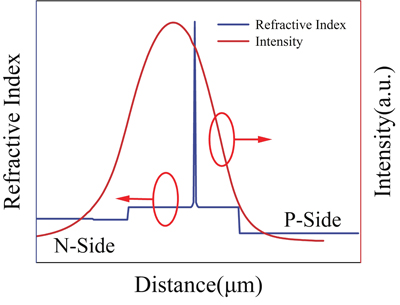
    Fig. 1. (Color online) Refractive index and light field distribution of the asymmetric large optical cavity structure.
    (Color online) Schematic diagram of the model for a single grating cycle
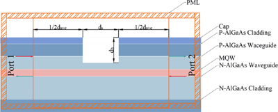
    Fig. 2. (Color online) Schematic diagram of the model for a single grating cycle
    (Color online) (a) The grating period and etch slot width versus grating transmittance for high precision scanning. (b) The grating period and etch slot width versus grating reflectance for high precision scanning.
    Fig. 3. (Color online) (a) The grating period and etch slot width versus grating transmittance for high precision scanning. (b) The grating period and etch slot width versus grating reflectance for high precision scanning.
    (Color online) (a) Relationship between etching depth and reflectivity for a grid period of 25. (b) Transmittance of gratings at different etching depths.
    Fig. 4. (Color online) (a) Relationship between etching depth and reflectivity for a grid period of 25. (b) Transmittance of gratings at different etching depths.
    (Color online) (a) Grating reflectance and transmittance versus grating period for a grating etching depth of 1.35 μm. (b) Transmittance of gratings at different grating period numbers.
    Fig. 5. (Color online) (a) Grating reflectance and transmittance versus grating period for a grating etching depth of 1.35 μm. (b) Transmittance of gratings at different grating period numbers.
    (Color online) (a) Effect of etch depth on threshold gain. (b) Effect of grating period on threshold gain.
    Fig. 6. (Color online) (a) Effect of etch depth on threshold gain. (b) Effect of grating period on threshold gain.
    SEM image after grid etching.
    Fig. 7. SEM image after grid etching.
    (Color online) (a) P−I−V curve of a HO-BDG-LD with 240 μm width; (b) P−I−V curve of a FP-LD without grating.
    Fig. 8. (Color online) (a) P−I−V curve of a HO-BDG-LD with 240 μm width; (b) P−I−V curve of a FP-LD without grating.
    Layer typeMaterialThickness (nm)
    ContactP-GaAs200
    P-claddingP-AlGaAs1000
    P-waveguideP-AlGaAs600
    QWInGaAs/AlGaAs
    N-waveguideN-AlGaAs900
    N-claddingN-AlGaAs1000
    BufferN-GaAs300
    SubstrateN-GaAs
    Table 0. Epitaxial structures of the laser diode.
    ParametersNumerical valueUnit
    L5500μm
    αi0.259[16]cm−1
    R20.99/
    Table 0. Parameters used in the calculation.
    Zhenwu Liu, Li Zhong, Suping Liu, Xiaoyu Ma. 975 nm multimode semiconductor lasers with high-order Bragg diffraction gratings[J]. Journal of Semiconductors, 2024, 45(3): 032401
    Download Citation