Journals > > Topics > Materials
Materials|31 Article(s)
Alkali Metal Ion, Gd3+, Ce3+ Co-doped Lu3Al5O12 Optical Properties of Ceramic Powder
Yunfeng BAI, Linxiang WANG, Qing LI, and [in Chinese]
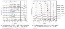
(GdxMyLu0.99-x-y)3Al5O12:1%Ce3+(x=0,0.01,0.25,0.5,0.75,y=0,0.005,0.01,0.02,0.05,0.1, M=Li+,Na+,K+,Cs+) series ceramic powders were synthesized by high temperature solid phase method. The microstructure of the sample was characterized by XRD, the excitation spectrum, emission spectrum and fluorescence lifetime of the sample were measured by FLS920 spectrometer, and the color coordinate of the sample was analyzed by the CIE chromaticity system. XRD results show that the Lu3Al5O12 samples co-doped with different concentrations of alkali metal ions、Gd3+ and Ce3+ are still cubic crystal phases, but with the increase of alkali metal ions, Gd3+ and Ce3+ doping concentrations, the diffraction peaks of the samples shift slightly to a small angle. Under the excitation of 350 nm, compared with the Lu2.97Al5O12:1%Ce3+ sample, the emission intensity of the sample co-doped with Gd3+ at around 511 nm decreased and appeared a significant red shift. With the increase of the doped Gd3+ concentration, the Ce3+ energy level lifetime gradually decreased. The range is 35~60 ns. Compared with the sample doped with 1%Ce3+ and 1%Gd3+, the luminescence intensity of the sample doped with 2%Li+, 2%Na+, 2%K+ and 1%Cs+ increased by 5.1 times and 2.93 times, respectively. At this time, the lifetime of Ce3+ in the sample continued to decrease. When the samples were irradiated under UV lamps with λ=254 nm and λ=365 nm, it was observed that with the increase of Gd3+ doping concentration, the color of the sample changed from dark yellow-green to dark red. The color coordinates show that the light-emitting area of the sample gradually moves from the yellow-green light area to the red light area. After co-doping with alkali metal ions, the sample emits brighter. (GdxMyLu0.99-x-y)3Al5O12:1%Ce3+(x=0,0.01,0.25,0.5,0.75,y=0,0.005,0.01,0.02,0.05,0.1, M=Li+,Na+,K+,Cs+) series ceramic powders were synthesized by high temperature solid phase method. The microstructure of the sample was characterized by XRD, the excitation spectrum, emission spectrum and fluorescence lifetime of the sample were measured by FLS920 spectrometer, and the color coordinate of the sample was analyzed by the CIE chromaticity system. XRD results show that the Lu3Al5O12 samples co-doped with different concentrations of alkali metal ions、Gd3+ and Ce3+ are still cubic crystal phases, but with the increase of alkali metal ions, Gd3+ and Ce3+ doping concentrations, the diffraction peaks of the samples shift slightly to a small angle. Under the excitation of 350 nm, compared with the Lu2.97Al5O12:1%Ce3+ sample, the emission intensity of the sample co-doped with Gd3+ at around 511 nm decreased and appeared a significant red shift. With the increase of the doped Gd3+ concentration, the Ce3+ energy level lifetime gradually decreased. The range is 35~60 ns. Compared with the sample doped with 1%Ce3+ and 1%Gd3+, the luminescence intensity of the sample doped with 2%Li+, 2%Na+, 2%K+ and 1%Cs+ increased by 5.1 times and 2.93 times, respectively. At this time, the lifetime of Ce3+ in the sample continued to decrease. When the samples were irradiated under UV lamps with λ=254 nm and λ=365 nm, it was observed that with the increase of Gd3+ doping concentration, the color of the sample changed from dark yellow-green to dark red. The color coordinates show that the light-emitting area of the sample gradually moves from the yellow-green light area to the red light area. After co-doping with alkali metal ions, the sample emits brighter.
Acta Photonica Sinica
- Publication Date: Apr. 25, 2021
- Vol. 50, Issue 4, 163 (2021)


Optically Transparent Hybrid Metasurfaces for Low Infrared Emission and Wideband Microwave Absorption
Cuilian XU, Yueyu MENG, Jiafu WANG, Mingbao YAN, Wenjie WANG, Jinming JIANG, and Shaobo QU
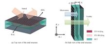
Based on the transparent conductive material Indium Tin Oxide (ITO) and highly transparent Polyethylene Terephthalate (PET), optically transparent ultra-wideband radar and infrared compatible stealth hybrid metasurfaces were achieved. Two specically designed optically transparent metasurfaces were combined to realize radar and IR bi-stealth. One was designed to control the microwave absorption though properly modifying the impedance and resonance peaks of the meta-atom. The other was empolyed to control the IR radiation.The absorptivity in the microwave band 8.0~32.0 GHz band is greater than 90%, and its infrared stealth performance and heat radiation characteristics are further studied. Based on the transparent conductive material Indium Tin Oxide (ITO) and highly transparent Polyethylene Terephthalate (PET), optically transparent ultra-wideband radar and infrared compatible stealth hybrid metasurfaces were achieved. Two specically designed optically transparent metasurfaces were combined to realize radar and IR bi-stealth. One was designed to control the microwave absorption though properly modifying the impedance and resonance peaks of the meta-atom. The other was empolyed to control the IR radiation.The absorptivity in the microwave band 8.0~32.0 GHz band is greater than 90%, and its infrared stealth performance and heat radiation characteristics are further studied.
Acta Photonica Sinica
- Publication Date: Apr. 25, 2021
- Vol. 50, Issue 4, 153 (2021)
Metal-assisted Low-energy Ar+ Ion Beam Induces Self-organized Nanostructure of Sapphire
Li TANG, Zhili CHEN, Yuzhao LIU, Qian BI, Yingxue XI, and Weiguo LIU
The plasma polishing and etching system independently developed by the laboratory was used to prepare sapphire self-organized nanostructures. The formation mechanism of self-organized nanostructures by Ar+ ion beam sputtering assisted with stainless steel at different incident energy was studied. The roughness, longitudinal height of nanostructure and surface morphology of the etched sapphire sample were respectively measured by Taylor Surf CCI2000 non-contact surface measuring instrument and atomic force microscope. With the ion beam incident angle of 65°, the beam current density of 487 μA/cm2, the etching time of 60 min, and the ion beam incident energy of 1 000 eV, well-ordered stripe-like nanostructures with a longitudinal height of 11.1 nm appear on the surface of the sapphire sample. As the incident energy increases, island-like nanostructures gradually appear on the surface of the substrate. When the incident energy is 1 200 eV, island-like structures and ripple generate on the substrate, with a longtidudinal height of 13.6 nm. With an increase of the incident energy, the density of island-like structures enhances. When the incident energy is 1 400 eV, the longitudinal height of island-like nanostructures is 18.8 nm.When the incident energy is 1 600 eV, the surface of the sapphire sample appears a relatively ordered island-like structure with a longitudinal height of 20.1 nm. During the ion beam sputtering process, with an increase of the incident energy, metal impurities break the balance between the surface growth mechanism and the surface smoothing mechanism, which form island-like nanostructures, these structures promote the growth of nanostructures and change the orderliness of nanostructures. The plasma polishing and etching system independently developed by the laboratory was used to prepare sapphire self-organized nanostructures. The formation mechanism of self-organized nanostructures by Ar+ ion beam sputtering assisted with stainless steel at different incident energy was studied. The roughness, longitudinal height of nanostructure and surface morphology of the etched sapphire sample were respectively measured by Taylor Surf CCI2000 non-contact surface measuring instrument and atomic force microscope. With the ion beam incident angle of 65°, the beam current density of 487 μA/cm2, the etching time of 60 min, and the ion beam incident energy of 1 000 eV, well-ordered stripe-like nanostructures with a longitudinal height of 11.1 nm appear on the surface of the sapphire sample. As the incident energy increases, island-like nanostructures gradually appear on the surface of the substrate. When the incident energy is 1 200 eV, island-like structures and ripple generate on the substrate, with a longtidudinal height of 13.6 nm. With an increase of the incident energy, the density of island-like structures enhances. When the incident energy is 1 400 eV, the longitudinal height of island-like nanostructures is 18.8 nm.When the incident energy is 1 600 eV, the surface of the sapphire sample appears a relatively ordered island-like structure with a longitudinal height of 20.1 nm. During the ion beam sputtering process, with an increase of the incident energy, metal impurities break the balance between the surface growth mechanism and the surface smoothing mechanism, which form island-like nanostructures, these structures promote the growth of nanostructures and change the orderliness of nanostructures.
Acta Photonica Sinica
- Publication Date: Feb. 25, 2021
- Vol. 50, Issue 2, 183 (2021)
Novel Huygens Metasurface with Capability of Anomalous Transmission
Xiaokun WANG, and Zhou LI
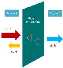
A novel Huygens particle, of which transmission magnitudes and phases can be controlled independently, is proposed here. The transmission magnitude can be arbitrarily tuned from 0 to 0.9, while the transmission phase is between 0 and 2π. Aligning Huygens particles based on generalized snell’s law, a metasurface structure with function of anomalous transmission is designed and fabricated. Full-wave simulation results prove that the plane electromagnetic wave normally incident from the bottom is nearly steered to 60° by the designed Huygens metasurface at 10 GHz. The near-field measurement results are basically consistent with the simulations, which demonstrates the correctness of desinged metasurface further. A novel Huygens particle, of which transmission magnitudes and phases can be controlled independently, is proposed here. The transmission magnitude can be arbitrarily tuned from 0 to 0.9, while the transmission phase is between 0 and 2π. Aligning Huygens particles based on generalized snell’s law, a metasurface structure with function of anomalous transmission is designed and fabricated. Full-wave simulation results prove that the plane electromagnetic wave normally incident from the bottom is nearly steered to 60° by the designed Huygens metasurface at 10 GHz. The near-field measurement results are basically consistent with the simulations, which demonstrates the correctness of desinged metasurface further.
Acta Photonica Sinica
- Publication Date: Feb. 25, 2021
- Vol. 50, Issue 2, 175 (2021)
Key Technologies of Microwave Wireless Power Transfer and Energy Harvesting Based on Electromagnetic Metamaterials(Invited)
Long LI, Pei ZHANG, Jiaqi HAN, and Tiejun CUI
1016001Wireless Power Transfer (WPT) and energy harvesting technologies are expected to provide revolutionary technological changes in important fields such as 5G communications and the Internet of Things. The short-range coupling WPT has gradually been commercialized, but there are still many technical bottlenecks in the practical process of microwave power transmission that can realize long-distance applications, such as the contradiction between the limited aperture of transceiver antennas and the WPT efficiency. The developments of electromagnetic metamaterials and metasurfaces have brought new breakthroughs for solving the above-mentioned problems. In this paper, we will focus on the combination of the two important technologies, and systematically review the applications of metamaterials in microwave wireless power transfer and wireless energy harvesting. The results show that the near-field focusing metasurface can significantly improve the transfer efficiency. We will also introduce the research progress of optically transparent metasurfaces and reconfigurable metasurfaces for improving WPT performance and practicability. Based on the periodically close arrangements of subwavelength metamaterial units, a wireless energy harvester with wide-angle incidence and polarization-insensitive characteristics is designed, which can replace conventional receiving antennas with higher harvesting efficiency. Furthermore, coplanar integration with the rectifying diodes makes a new concept of the rectifying metasurface, which can simplify the overall structure, reduce the size, and improve the efficiency. Finally, we will discuss the future progress of WPT, and point out the vital role that programmable and intelligent metamaterial technologies will play very important roles in future simultaneous wireless information and power transfer systems. 1016001Wireless Power Transfer (WPT) and energy harvesting technologies are expected to provide revolutionary technological changes in important fields such as 5G communications and the Internet of Things. The short-range coupling WPT has gradually been commercialized, but there are still many technical bottlenecks in the practical process of microwave power transmission that can realize long-distance applications, such as the contradiction between the limited aperture of transceiver antennas and the WPT efficiency. The developments of electromagnetic metamaterials and metasurfaces have brought new breakthroughs for solving the above-mentioned problems. In this paper, we will focus on the combination of the two important technologies, and systematically review the applications of metamaterials in microwave wireless power transfer and wireless energy harvesting. The results show that the near-field focusing metasurface can significantly improve the transfer efficiency. We will also introduce the research progress of optically transparent metasurfaces and reconfigurable metasurfaces for improving WPT performance and practicability. Based on the periodically close arrangements of subwavelength metamaterial units, a wireless energy harvester with wide-angle incidence and polarization-insensitive characteristics is designed, which can replace conventional receiving antennas with higher harvesting efficiency. Furthermore, coplanar integration with the rectifying diodes makes a new concept of the rectifying metasurface, which can simplify the overall structure, reduce the size, and improve the efficiency. Finally, we will discuss the future progress of WPT, and point out the vital role that programmable and intelligent metamaterial technologies will play very important roles in future simultaneous wireless information and power transfer systems.
Acta Photonica Sinica
- Publication Date: Oct. 25, 2021
- Vol. 50, Issue 10, 1016001 (2021)

Free Manipulation of Terahertz Wave Based on the Transmission Type Geometric Phase Coding Metasurface
Xiaoyan TANG, Youhuang KE, Xufeng JING, Xun BIE, Chenxia LI, and Zhi HONG
In order to realize the free manipulation of terahertz beams, a multi-layer C-type unit structure is proposed to realize the phase control of the transmissionterahertz waves from 0 to 2π at the target frequency based on the Pancharatnam-Berry geometric phase theory. Based on the generalized Snell's law, 2-bit and 3-bit coding metasurfaces are constructed. The scattering angle of the transmissive terahertz beam can be controlled with the incidence of circular polarization wave. By using the Fourier convolution operation in the digital signal processing theory, the four-bit encoding convolution operation is performed on the coding metasurfaces of different periodic sequences to obtain a new coding sequence and realize the free adjustment of the transmission angle of the terahertz wave. The multi-layer C-encoded metasurface unit structure is used to perform rotary encoding to realize the 1st and 2nd order vortex phase plates and generate different orders of terahertz wave vortex beams. In order to realize the free manipulation of terahertz beams, a multi-layer C-type unit structure is proposed to realize the phase control of the transmissionterahertz waves from 0 to 2π at the target frequency based on the Pancharatnam-Berry geometric phase theory. Based on the generalized Snell's law, 2-bit and 3-bit coding metasurfaces are constructed. The scattering angle of the transmissive terahertz beam can be controlled with the incidence of circular polarization wave. By using the Fourier convolution operation in the digital signal processing theory, the four-bit encoding convolution operation is performed on the coding metasurfaces of different periodic sequences to obtain a new coding sequence and realize the free adjustment of the transmission angle of the terahertz wave. The multi-layer C-encoded metasurface unit structure is used to perform rotary encoding to realize the 1st and 2nd order vortex phase plates and generate different orders of terahertz wave vortex beams.
Acta Photonica Sinica
- Publication Date: Jan. 25, 2021
- Vol. 50, Issue 1, 142 (2021)
Terahertz Microfluidic Sensor Based on Metamaterial Absorbers with Enhanced Electromagnetic Field Interaction
Tao CHEN, Fengyu HUANG, Xin ZHONG, Weijie JIANG, and Dapeng ZHANG
To solve the problem of the limited sensitivity, which is due to the poor interaction between the analytes and the localized enhanced electromagnetic field, the terahertz microfluidic sensor based on a metamaterial absorber with the enhanced electromagnetic field interaction is proposed by introducing the microfluidics technology. Owing to the interaction of the sensor and terahertz waves, the magnetic dipole resonances are excited and two significant absorption peaks with the absorption rates over 98% are formed in the range of 0.4~1.4 THz. Meanwhile, with integrating the microfluidic channel, the interaction between the analytes and the localized enhanced electromagnetic field located in the Fabry-Pérot cavity is dramatically enhanced, and the sensor can reach the high sensitivity of 537 GHz/RIU. In addition, the unit cell is designed as the four-fold rotational symmetrical structure, so that the polarization-insensitivitive and the wide range of incident-angle-insensitive properties of the sensor are obtained. The results indicate that the proposed sensor has the characteristics of high sensitivity and polarization-independent, and it exhibits a promising application prospect in the field of label-free trace detection. To solve the problem of the limited sensitivity, which is due to the poor interaction between the analytes and the localized enhanced electromagnetic field, the terahertz microfluidic sensor based on a metamaterial absorber with the enhanced electromagnetic field interaction is proposed by introducing the microfluidics technology. Owing to the interaction of the sensor and terahertz waves, the magnetic dipole resonances are excited and two significant absorption peaks with the absorption rates over 98% are formed in the range of 0.4~1.4 THz. Meanwhile, with integrating the microfluidic channel, the interaction between the analytes and the localized enhanced electromagnetic field located in the Fabry-Pérot cavity is dramatically enhanced, and the sensor can reach the high sensitivity of 537 GHz/RIU. In addition, the unit cell is designed as the four-fold rotational symmetrical structure, so that the polarization-insensitivitive and the wide range of incident-angle-insensitive properties of the sensor are obtained. The results indicate that the proposed sensor has the characteristics of high sensitivity and polarization-independent, and it exhibits a promising application prospect in the field of label-free trace detection.
Acta Photonica Sinica
- Publication Date: Jan. 25, 2021
- Vol. 50, Issue 1, 131 (2021)
Crystallization Mechanism of Photo-thermal-refractive Glass in SiO2-Al2O3-ZnO-Na2O(F, Br) System
Zi-wei XU, Bao-xing XIONG, Zhao-wen CAO, and Kuai-sheng ZOU
The volume Bragg grating was prepared by using the "five-step" thermal fixing process, crystallization mechanism of the photo-thermo-rraphictive glass is described, and the ion migration process and NaF crystallization process are intuitively detected by Raman spectroscopy and scanning electron microscopy. The absorption band at 350~600 nm is found by transmission spectrum, and the colloid formed in the internal nucleation process is determined to be a silver bromide and silver nanocomposite.The key factors influencing the crystallized particles in photo-thermal-refractive glass were investigated from three aspects:nucleation process, NaF crystallization process and UV exposure dosage. It is found that the size of[Agn0·(AgBr)m] micelles is the key to determine the crystal size of NaF during nucleation. The crystallization process mainly affects the number of crystal particles and has little effect on changing the crystal size.As the exposure dosage increases, the crystallization size of NaF decreases first and then increases, the inflection point is around 1.8 J/cm2, and the crystalline particles are the smallest. The volume Bragg grating was prepared by using the "five-step" thermal fixing process, crystallization mechanism of the photo-thermo-rraphictive glass is described, and the ion migration process and NaF crystallization process are intuitively detected by Raman spectroscopy and scanning electron microscopy. The absorption band at 350~600 nm is found by transmission spectrum, and the colloid formed in the internal nucleation process is determined to be a silver bromide and silver nanocomposite.The key factors influencing the crystallized particles in photo-thermal-refractive glass were investigated from three aspects:nucleation process, NaF crystallization process and UV exposure dosage. It is found that the size of[Agn0·(AgBr)m] micelles is the key to determine the crystal size of NaF during nucleation. The crystallization process mainly affects the number of crystal particles and has little effect on changing the crystal size.As the exposure dosage increases, the crystallization size of NaF decreases first and then increases, the inflection point is around 1.8 J/cm2, and the crystalline particles are the smallest.
Acta Photonica Sinica
- Publication Date: Aug. 25, 2020
- Vol. 49, Issue 7, 716002 (2020)
Luminous Properties of near Infrared Excited Upconversion Luminescent Materials Based on NaYF4
Dong-dong LI, Tian YANG, Xin-yu MA, Dong-dong HAN, and Jiang-bo SHE
NaYF4:Yb3+/Tb3+ and NaYF4:Yb3+/Tm3+ double doping fluoride nanomaterials with different doping concentrations were prepared by hydrothermal synthesis. In these materials, the Yb3+ was used as sensitizer to assist in luminous, Tb3+ and Tm3+ were added to the matrix sodium yttrium fluoride as activators of luminous center. The morphology and luminous properties of NaYF4:Yb3+/Tb3+ and NaYF4:Yb3+/Tm3+ nanoparticles were investigated by scanning electron microscope (SEM), X-ray diffraction andfluorescence spectrum. The X-ray diffraction patterns of the series of samples well match the NaYF4 standard card. Upconversion luminescence spectra of materials under 980 nm laser excitation were obtained and the mechanism was also analyzed. Excited by 980 nm laser, the emission spectra of NaYF4:Yb3+/Tb3+ including blue, green and red light, which correspond to the radiative transition of 5D4→7F6, 5D4→7F5, 5D4→7F1, respectively. The strong 480 nm emission can be seen in NaYF4:Yb3+/Tm3+ excited by 980 nm laser, corresponding to the electron transition energy band of 1G4→3H6. A strong red light emission band centered at 660 nm is corresponding to the 1G4→3F4 energy level transition. NaYF4:Yb3+/Tb3+ and NaYF4:Yb3+/Tm3+ double doping fluoride nanomaterials with different doping concentrations were prepared by hydrothermal synthesis. In these materials, the Yb3+ was used as sensitizer to assist in luminous, Tb3+ and Tm3+ were added to the matrix sodium yttrium fluoride as activators of luminous center. The morphology and luminous properties of NaYF4:Yb3+/Tb3+ and NaYF4:Yb3+/Tm3+ nanoparticles were investigated by scanning electron microscope (SEM), X-ray diffraction andfluorescence spectrum. The X-ray diffraction patterns of the series of samples well match the NaYF4 standard card. Upconversion luminescence spectra of materials under 980 nm laser excitation were obtained and the mechanism was also analyzed. Excited by 980 nm laser, the emission spectra of NaYF4:Yb3+/Tb3+ including blue, green and red light, which correspond to the radiative transition of 5D4→7F6, 5D4→7F5, 5D4→7F1, respectively. The strong 480 nm emission can be seen in NaYF4:Yb3+/Tm3+ excited by 980 nm laser, corresponding to the electron transition energy band of 1G4→3H6. A strong red light emission band centered at 660 nm is corresponding to the 1G4→3F4 energy level transition.
Acta Photonica Sinica
- Publication Date: Aug. 25, 2020
- Vol. 49, Issue 7, 716001 (2020)
Photoluminescence Spectrum of Monolayer MoSe2 Tuned by Strain
Han LIAO, Xiao-juan SHE, Lue TAO, Yang LI, Jia-xiang ZHANG, Fu-wan GAN, and Zhi LIU
In order to explore the potential of 2D materials in the application field of on-chip tunable active optical devices, a strain-tunable light source with monolayer MoSe2 was produced. High quality monolayer MoSe2 was obtained by micromechanical exfoliation method. The all-dry transfer method was used to transfer monolayer MoSe2 to biaxial piezoelectric ceramics coated with 150 nm thick Polymethylmethacrylate. The electric field was applied to the biaxial piezoelectric ceramic, which converts the electrical signal into the strain signal, to controll the optical properties of MoSe2. The variation of intrinsic exciton and charge exciton peaks of the MoSe2 with strain tuning were observed from photoluminescence spectra at low temperature of~5 K. The results indicate that blueshifts of ~3.8 meV and ~3.7 meV appear in the intrinsic exciton and charge exciton peaks, respectively, when the strain is tuned from tension to compression. And increasing compressive strain or tensile strain will decrease the intensity of intrinsic exciton and charge exciton peak linearly. At the same time, the circular polarization degree of the emission related to the circular polarization of the pump laser also shows regular change with the variation of strain. This research confirms the close correlation between the stain tuning and the optical properties of monolayer MoSe2. It provides support for the development of various on-chip tunable active optical devices based on 2D materials. In order to explore the potential of 2D materials in the application field of on-chip tunable active optical devices, a strain-tunable light source with monolayer MoSe2 was produced. High quality monolayer MoSe2 was obtained by micromechanical exfoliation method. The all-dry transfer method was used to transfer monolayer MoSe2 to biaxial piezoelectric ceramics coated with 150 nm thick Polymethylmethacrylate. The electric field was applied to the biaxial piezoelectric ceramic, which converts the electrical signal into the strain signal, to controll the optical properties of MoSe2. The variation of intrinsic exciton and charge exciton peaks of the MoSe2 with strain tuning were observed from photoluminescence spectra at low temperature of~5 K. The results indicate that blueshifts of ~3.8 meV and ~3.7 meV appear in the intrinsic exciton and charge exciton peaks, respectively, when the strain is tuned from tension to compression. And increasing compressive strain or tensile strain will decrease the intensity of intrinsic exciton and charge exciton peak linearly. At the same time, the circular polarization degree of the emission related to the circular polarization of the pump laser also shows regular change with the variation of strain. This research confirms the close correlation between the stain tuning and the optical properties of monolayer MoSe2. It provides support for the development of various on-chip tunable active optical devices based on 2D materials.
Acta Photonica Sinica
- Publication Date: Jun. 25, 2020
- Vol. 49, Issue 6, 0616002 (2020)
Topics
© Copyright 2018-2021 | Chinese Laser Press. All Rights Reserved 沪ICP备15018463号-20