Journals > > Topics > Optoelectronics
Optoelectronics|112 Article(s)
Design and Modulation Performance of Ultrafast Light-controlled Pulsed X-ray Tube with Photocathode
Hao XUAN, Yongan LIU, Pengfei QIANG, Tong SU, Xianghui YANG, Lizhi SHENG, and Baosheng ZHAO
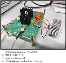
In order to solve the easy-broken structure, low energy efficiency and heat dissipation of the traditional X-ray tube with filament based on thermionic cathode, a novel light-controlled pulsed X-ray tube device is deostrated in this paper. By matching the parameters of photocathode and light source, S20 cathode with high quantum efficiency and LED with 460 nm wavelength were selected. At the same time, the overall structure design of the X-ray tube is determined by the simulation. Finally, the maximum tube current of 2.37 mA is realized, the electron emission efficiency of photocathode is 0.288 mA/lm, and the output X-ray energy is adjustable from 0 to 25 keV. In addition, based on the characteristics of easy-access to be modulated of the light-controlled pulsed X-ray tube, different frequencies input signal restoration experiment and arbitrary contor X-ray restoration experiment was carried out. In order to solve the easy-broken structure, low energy efficiency and heat dissipation of the traditional X-ray tube with filament based on thermionic cathode, a novel light-controlled pulsed X-ray tube device is deostrated in this paper. By matching the parameters of photocathode and light source, S20 cathode with high quantum efficiency and LED with 460 nm wavelength were selected. At the same time, the overall structure design of the X-ray tube is determined by the simulation. Finally, the maximum tube current of 2.37 mA is realized, the electron emission efficiency of photocathode is 0.288 mA/lm, and the output X-ray energy is adjustable from 0 to 25 keV. In addition, based on the characteristics of easy-access to be modulated of the light-controlled pulsed X-ray tube, different frequencies input signal restoration experiment and arbitrary contor X-ray restoration experiment was carried out.
Acta Photonica Sinica
- Publication Date: Jul. 25, 2021
- Vol. 50, Issue 7, 195 (2021)


Measure and Comparison between the Second-generation and the Third-generation Image Intensifier within the Different Region of Wavelength
Xiaofeng LI, Jiaojiao LI, Jinsha LI, Yaohong QIAN, Tianning SU, and Qiang WANG
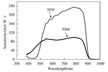
The spectral response, cathode sensitivity, gain, resolution and signal-to-noise ratio of the super second-generation and the third-generation image intensifier were measured at the short wave cut-off of 550 nm, 625 nm and 675 nm for A luminant. Under 10-1 lx illumination, the resolution of the third-generation image intensifier does not decrease after undertaking 675 nm short wave cut-off for A luminant, while the resolution of super second-generation image intensifier drops to 94% of the initial value; however, under 10-4 lx illumination, the resolution of the third-generation image intensifier decreases to 90% of the initial value after undertaking 675 nm short wave cut-off for the A luminant, while that of the super second-generation image intensifier decreases to 85%of the initial value. In addition, the resolution decreases with the decrease of illumination. For the super second-generation and third-generation image intensifiers, although the parameters are the same under the illumination of A luminant, but when used in different short wave cut-off wavelengths, the performance of the third-generation image intensifier is better. Although the decline proportion of parameters for super second-generation image intensifier is higher than that of third-generation image intensifier under different short wave cut-off wavelengths, the difference is not obvious, so the performance difference during use is not obvious. The spectral response, cathode sensitivity, gain, resolution and signal-to-noise ratio of the super second-generation and the third-generation image intensifier were measured at the short wave cut-off of 550 nm, 625 nm and 675 nm for A luminant. Under 10-1 lx illumination, the resolution of the third-generation image intensifier does not decrease after undertaking 675 nm short wave cut-off for A luminant, while the resolution of super second-generation image intensifier drops to 94% of the initial value; however, under 10-4 lx illumination, the resolution of the third-generation image intensifier decreases to 90% of the initial value after undertaking 675 nm short wave cut-off for the A luminant, while that of the super second-generation image intensifier decreases to 85%of the initial value. In addition, the resolution decreases with the decrease of illumination. For the super second-generation and third-generation image intensifiers, although the parameters are the same under the illumination of A luminant, but when used in different short wave cut-off wavelengths, the performance of the third-generation image intensifier is better. Although the decline proportion of parameters for super second-generation image intensifier is higher than that of third-generation image intensifier under different short wave cut-off wavelengths, the difference is not obvious, so the performance difference during use is not obvious.
Acta Photonica Sinica
- Publication Date: Feb. 25, 2021
- Vol. 50, Issue 2, 115 (2021)
Study on the Relationship between Noise Factor and Working Voltage of Microchannel Plate
Xiao-feng LI, Jin-sha LI, Le CHANG, Jiao-jiao LI, Jin-neng ZENG, and Yong-xiang WU
In order to work out the measuring method of noise factor of microchannel plate, a method to measure the noise factor of microchannel plate by measuring the sensitivity of photocathode and signal to noise ratio of image intensifier is proposed. According to this method, the noise factor of microchannel plate is measured under different cathode voltage, microchannel plate voltage and anode voltage. The results show that the noise factor of microchannel plate change with the change of cathode voltage, microchannel plate voltage and anode voltage. The voltage of microchannel plate has the greatest influence on noise factor and the anode voltage has the least. When the voltage of microchannel plate is increased by 100 V, the noise factor increases by about 0.11. The noise factor increases about 3.3×10⁻⁴ for every 100 V of anode voltage. The increase of working voltage of microchannel plate means the increase of electron collision energy and the increase of secondary electron emission coefficient. According to the existing noise theory of microchannel plate, the noise factor of microchannel plate will be reduced, but the measured results are increased. The reason for this contradiction is that in the existing noise theory of microchannel plate, only the influence of secondary electron emission coefficient, detection rate and electron collision probability on the noise factor are considered, but the influence of collision electron energy on the noise factor is not considered, so the noise theory needs to be revised. In order to work out the measuring method of noise factor of microchannel plate, a method to measure the noise factor of microchannel plate by measuring the sensitivity of photocathode and signal to noise ratio of image intensifier is proposed. According to this method, the noise factor of microchannel plate is measured under different cathode voltage, microchannel plate voltage and anode voltage. The results show that the noise factor of microchannel plate change with the change of cathode voltage, microchannel plate voltage and anode voltage. The voltage of microchannel plate has the greatest influence on noise factor and the anode voltage has the least. When the voltage of microchannel plate is increased by 100 V, the noise factor increases by about 0.11. The noise factor increases about 3.3×10⁻⁴ for every 100 V of anode voltage. The increase of working voltage of microchannel plate means the increase of electron collision energy and the increase of secondary electron emission coefficient. According to the existing noise theory of microchannel plate, the noise factor of microchannel plate will be reduced, but the measured results are increased. The reason for this contradiction is that in the existing noise theory of microchannel plate, only the influence of secondary electron emission coefficient, detection rate and electron collision probability on the noise factor are considered, but the influence of collision electron energy on the noise factor is not considered, so the noise theory needs to be revised.
Acta Photonica Sinica
- Publication Date: Aug. 25, 2020
- Vol. 49, Issue 7, 725002 (2020)
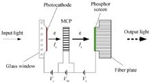
Inductive Charge Readout for Far Ultraviolet Photon Count Imaging Detector
Ke-fei SONG, Zhen-wei HAN, Ling-ping HE, and Qi-liang NI
In order to meet the need of high spatial resolution and high count rate in the imaging of far ultraviolet band, the method of acquiring the induced charge of the photon count imaging detector is described, which can be used in the imaging spectrometer for remote sensing of far ultraviolet band in the ionosphere of the earth. The relation between the parameters of the charge sensitive amplifier with pulse shaper is studied. The influence of the rise time of the charge sensitive amplifier and the time constant of the pulse shaper on the noise and counting rate is analyzed by numerical model. The selection principle of network parameters is proposed, and a front-end readout circuitry for photon count imaging detector based on wedge and strip anode is developed with discrete electronic components suitable for space applications. The experiment results show that when the shaping time is 500 ns, the equivalent input noise charge of readout circuits is about 230 e, and the rise time of the charge sensitive amplifier is better than 8 ns, which have better consistency with the calculated values. The spatial resolution of the measured images is up to 7.13 lp/mm, and the highest counting rate is 86.2 kcps, which meets the requirements of the far-ultraviolet band imaging spectrometer on-orbit mission operations. In order to meet the need of high spatial resolution and high count rate in the imaging of far ultraviolet band, the method of acquiring the induced charge of the photon count imaging detector is described, which can be used in the imaging spectrometer for remote sensing of far ultraviolet band in the ionosphere of the earth. The relation between the parameters of the charge sensitive amplifier with pulse shaper is studied. The influence of the rise time of the charge sensitive amplifier and the time constant of the pulse shaper on the noise and counting rate is analyzed by numerical model. The selection principle of network parameters is proposed, and a front-end readout circuitry for photon count imaging detector based on wedge and strip anode is developed with discrete electronic components suitable for space applications. The experiment results show that when the shaping time is 500 ns, the equivalent input noise charge of readout circuits is about 230 e, and the rise time of the charge sensitive amplifier is better than 8 ns, which have better consistency with the calculated values. The spatial resolution of the measured images is up to 7.13 lp/mm, and the highest counting rate is 86.2 kcps, which meets the requirements of the far-ultraviolet band imaging spectrometer on-orbit mission operations.
Acta Photonica Sinica
- Publication Date: Aug. 25, 2020
- Vol. 49, Issue 7, 725001 (2020)
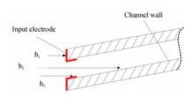
Study on the Improvement of Input Signal Utilization of MCP
Xiao-feng LI, Ting-tao LI, Jin-neng ZENG, Le CHANG, and Chao CHEN
In this paper, the reason of input signal loss caused by input electrode of Microchannel Plate (MCP) is analyzed, and a method of plating insulation layer on input end of MCP is proposed to increase the utilization of input signal of MCP which is verified by experiment. The experimental results show that a layer of 15 nm thick insulating layer is plated on the input end of the MCP, which can increase the utilization of the input signal of the MCP and the gain of the MCP. The higher the secondary electron emission coefficient of the insulating layer is, the higher the utilization ratio of the input signal of the MCP is, and the larger the ratio of the gain increase is. For SiO2 films, the gain can be increased by about 12%. For Al2O3 films, the gain can be increased by about 35%. At the same time, the resolution and MTF of image intensifier will decrease slightly. Similarly, the higher the secondary electron emission coefficient is, the larger the decrease ratio of resolution and MTF is. However, the decrease ratio of resolution and MTF of MCP is much lower than that of gain increase. The method proposed in this paper to increase the utilization rate of input signal of MCP has certain practicability and can be popularized. In this paper, the reason of input signal loss caused by input electrode of Microchannel Plate (MCP) is analyzed, and a method of plating insulation layer on input end of MCP is proposed to increase the utilization of input signal of MCP which is verified by experiment. The experimental results show that a layer of 15 nm thick insulating layer is plated on the input end of the MCP, which can increase the utilization of the input signal of the MCP and the gain of the MCP. The higher the secondary electron emission coefficient of the insulating layer is, the higher the utilization ratio of the input signal of the MCP is, and the larger the ratio of the gain increase is. For SiO2 films, the gain can be increased by about 12%. For Al2O3 films, the gain can be increased by about 35%. At the same time, the resolution and MTF of image intensifier will decrease slightly. Similarly, the higher the secondary electron emission coefficient is, the larger the decrease ratio of resolution and MTF is. However, the decrease ratio of resolution and MTF of MCP is much lower than that of gain increase. The method proposed in this paper to increase the utilization rate of input signal of MCP has certain practicability and can be popularized.
Acta Photonica Sinica
- Publication Date: Mar. 25, 2020
- Vol. 49, Issue 3, 0325002 (2020)

Measurement of Quantum Yield and Image of Microchannel Plate in Near Ultraviolet Band
Xiao-feng LI, Le CHANG, Yong-sheng QIU, Yong-xiang WU, and Yong-chun LI
A method is proposed to calculate the photocurrent by measuring the output current and gain of microchannel plate, so as to measure the quantum yield. The quantum yield is measured in the near ultraviolet (200~380 nm) by the proposed method. The measurement results show that the quantum yield of microchannel plate is very low, and decreases rapidly with the increase of wavelength. The quantum yield of 200 nm wavelength is 10-4 order of magnitude; the quantum yield of 320 nm wavelength is 10-8 order of magnitude, and the quantum yield after 340 nm wavelength is very low and almost zero. The imaging device composed of microchannel plate and fluorescent screen can image the flame of alcohol lighter, but the image is sparse, while the image of traditional Cs2 Te photocathode ultraviolet imaging device is dense, which is consistent with the situation of low quantum yield of microchannel plate and high quantum yield of Cs2 Te photocathode. When a 350 nm high pass filter is placed at the front of the imaging device, the detected flame image of the alcohol lighter disappears. When imaging the illuminated target, it can be imaged if the light source is a 254 nm mercury lamp; but it cannot be imaged, if the light source is a 365 nm mercury lamp. The results show that the spectral response of microchannel plate is mainly below 350 nm wavelength, which is consistent with the measurement results of quantum yield. Finally, the resolution of the imaging device is measured as 32 lp/mm, which is the same as that of the traditional Cs2 Te photocathode ultraviolet imaging device. Because the imaging device composed of microchannel plate and fluorescent screen does not use photocathode, it has the advantages of low price, long life and high reliability, so it can be used under the condition of strong ultraviolet signal or short imaging distance. A method is proposed to calculate the photocurrent by measuring the output current and gain of microchannel plate, so as to measure the quantum yield. The quantum yield is measured in the near ultraviolet (200~380 nm) by the proposed method. The measurement results show that the quantum yield of microchannel plate is very low, and decreases rapidly with the increase of wavelength. The quantum yield of 200 nm wavelength is 10-4 order of magnitude; the quantum yield of 320 nm wavelength is 10-8 order of magnitude, and the quantum yield after 340 nm wavelength is very low and almost zero. The imaging device composed of microchannel plate and fluorescent screen can image the flame of alcohol lighter, but the image is sparse, while the image of traditional Cs2 Te photocathode ultraviolet imaging device is dense, which is consistent with the situation of low quantum yield of microchannel plate and high quantum yield of Cs2 Te photocathode. When a 350 nm high pass filter is placed at the front of the imaging device, the detected flame image of the alcohol lighter disappears. When imaging the illuminated target, it can be imaged if the light source is a 254 nm mercury lamp; but it cannot be imaged, if the light source is a 365 nm mercury lamp. The results show that the spectral response of microchannel plate is mainly below 350 nm wavelength, which is consistent with the measurement results of quantum yield. Finally, the resolution of the imaging device is measured as 32 lp/mm, which is the same as that of the traditional Cs2 Te photocathode ultraviolet imaging device. Because the imaging device composed of microchannel plate and fluorescent screen does not use photocathode, it has the advantages of low price, long life and high reliability, so it can be used under the condition of strong ultraviolet signal or short imaging distance.
Acta Photonica Sinica
- Publication Date: Mar. 25, 2020
- Vol. 49, Issue 3, 0325001 (2020)
Study of Electronic Transport Characteristic and Electric Field Enhancement Effect of Wafer-bonded Si/Si p-n Junction
Qiang PENG, Sheng-quan HE, Liang-bin REN, Xing-lian LI, and Shao-ying KE
Although high-strength and bubble-free Si/Si wafer pairs can be obtained by the Si/Si wafer bonding, the oxide-layer-free Si/Si bonded interface is difficult to be achieved. Thus, the Si/Si wafer bonding is difficult to be used in the field of optoelectronics. The effect of oxide layer thickness on the photoelectric characteristics (current, bandwidth, and spectrum) of wafer-bonded Si/Si p-n junction is studied. The factors which affect the performance of the Si/Si p-n junction are clarified by the simulation of carrier tunneling rate, carrier concentration, electric field, carrier velocity, and recombination rate. This may give guidance for the fabrication of ultrahigh-quality Si-based Si avalanche layer and high-performance Si-based avalanche device. The simulation results show that: with the increase of the oxide layer thickness, the carrier tunneling rate decreases, leading to the decrease of the dark current and photocurrent. The recombination rate also decreases and the carriers aggregate in the p-n junction. In addition, with the increase of the oxide layer thickness, the RC time constant of the device increases and the electric field enhances in the oxide layer, leading to the decrease of the electric field, which in turn results in the decrease of the 3 dB bandwidth. Although high-strength and bubble-free Si/Si wafer pairs can be obtained by the Si/Si wafer bonding, the oxide-layer-free Si/Si bonded interface is difficult to be achieved. Thus, the Si/Si wafer bonding is difficult to be used in the field of optoelectronics. The effect of oxide layer thickness on the photoelectric characteristics (current, bandwidth, and spectrum) of wafer-bonded Si/Si p-n junction is studied. The factors which affect the performance of the Si/Si p-n junction are clarified by the simulation of carrier tunneling rate, carrier concentration, electric field, carrier velocity, and recombination rate. This may give guidance for the fabrication of ultrahigh-quality Si-based Si avalanche layer and high-performance Si-based avalanche device. The simulation results show that: with the increase of the oxide layer thickness, the carrier tunneling rate decreases, leading to the decrease of the dark current and photocurrent. The recombination rate also decreases and the carriers aggregate in the p-n junction. In addition, with the increase of the oxide layer thickness, the RC time constant of the device increases and the electric field enhances in the oxide layer, leading to the decrease of the electric field, which in turn results in the decrease of the 3 dB bandwidth.
Acta Photonica Sinica
- Publication Date: Dec. 28, 2020
- Vol. 49, Issue 10, 1025002 (2020)
Multiplying Organic Photodetector Based on Double-doped C60:DDQ Trap
Tao AN, Xi-mei WU, and Xin-ying LIU
Organic photomultiplier detector with high trap concentration is developed by double doping method. By keeping the optimal doping ratio of C60 unchanged (1.0 wt%) based on the optimized single-doped device (active layer is P3HT:PC61BM:C60), while doping both C60 and DDQ electron traps, the effects of different DDQ doping concentrations on the trap concentration of the P3HT:PC61BM active layer and the photoelectric performance of the detector are studied.The study shows that the maximum doping concentration of the double-doped C60:DDQ active layer was 1.5 wt%, which is about 1.5 times higher than that of the single-doped C60 active layer (maximum doping concentration is 1.0 wt%). The trap concentration of the double-doped C60:DDQ device is 2.02×1018 cm-3, which is about 3.5 times higher than that of the single-doped C60 device (trap concentration is 5.83×1017 cm-3). Under the bias voltage of -2 V, the external quantum efficiency of the double-doped C60:DDQ device is as high as 2015.32%, which is about 10 times higher than that of the single-doped C60 device (external quantum efficiency is 202.60%). The results show that the double doping method can greatly increase the trap concentration, so as to realize the high concentration trap doping of the active layer. Organic photomultiplier detector with high trap concentration is developed by double doping method. By keeping the optimal doping ratio of C60 unchanged (1.0 wt%) based on the optimized single-doped device (active layer is P3HT:PC61BM:C60), while doping both C60 and DDQ electron traps, the effects of different DDQ doping concentrations on the trap concentration of the P3HT:PC61BM active layer and the photoelectric performance of the detector are studied.The study shows that the maximum doping concentration of the double-doped C60:DDQ active layer was 1.5 wt%, which is about 1.5 times higher than that of the single-doped C60 active layer (maximum doping concentration is 1.0 wt%). The trap concentration of the double-doped C60:DDQ device is 2.02×1018 cm-3, which is about 3.5 times higher than that of the single-doped C60 device (trap concentration is 5.83×1017 cm-3). Under the bias voltage of -2 V, the external quantum efficiency of the double-doped C60:DDQ device is as high as 2015.32%, which is about 10 times higher than that of the single-doped C60 device (external quantum efficiency is 202.60%). The results show that the double doping method can greatly increase the trap concentration, so as to realize the high concentration trap doping of the active layer.
Acta Photonica Sinica
- Publication Date: Oct. 15, 2020
- Vol. 49, Issue 10, 1025001 (2020)
Detection Performance for Laser Radars that Use Geiger-mode APD in Atmosphere Background
SU Bi-da, WANG Jing-feng, MA Xue-song, ZHANG Hai-yang, HUA Hao, and YANG Su-hui
The Geiger-mode APD is very sensitive. For this advantages, it is widely used for astro-observation, particle physics, LIDAR. Sky background noise is a big problem for Geiger-mode APD detector during the day. The detection statistical model in theory was built, False alarm probability and detection probability and finding the way to increase maximum detection distance in difference detection threshold and background noise were discussed. In difference background noise, the maximum detection distance was determined. By limiting the filter bandwidth or reducing the detector open time, the background noise photon number is reduced to 2. The success rate of detection at 900Km is 96.6%. To the non-cooperative target, when the radar scattering cross section is 1 m2, the success rate of detection is 70%. The Geiger-mode APD is very sensitive. For this advantages, it is widely used for astro-observation, particle physics, LIDAR. Sky background noise is a big problem for Geiger-mode APD detector during the day. The detection statistical model in theory was built, False alarm probability and detection probability and finding the way to increase maximum detection distance in difference detection threshold and background noise were discussed. In difference background noise, the maximum detection distance was determined. By limiting the filter bandwidth or reducing the detector open time, the background noise photon number is reduced to 2. The success rate of detection at 900Km is 96.6%. To the non-cooperative target, when the radar scattering cross section is 1 m2, the success rate of detection is 70%.
Acta Photonica Sinica
- Publication Date: Jan. 01, 2015
- Vol. 44, Issue 1, 125003 (2015)
The Research of Balance Detector for High-speed Coherence Optical Communications
DAI Yong-hong, AI Yong, XIAO Wei, ZHOU Hao-tian, and SHAN Xin
The principle and key technology of balance detcetor for coherent optical communication were analyzed.A set of high-speed balance detection system was designed,and the coherent optical communications test platform was built indoors.Actual tests show that the balance detector can achieve the different rate of coherent detection,which can provide an essential support for coherent optical communication.Under 2.5 Gbps,the sensitivity can be obtained -26 dBm under the condition of direct detection using single pipe,where dynamic range is -26-3 dBm.When the power of local oscillator laser is 3dBm,coherent detection sensitivity can reach 46.5 dBm,where dynamic range is -46.5-3 dBm. The principle and key technology of balance detcetor for coherent optical communication were analyzed.A set of high-speed balance detection system was designed,and the coherent optical communications test platform was built indoors.Actual tests show that the balance detector can achieve the different rate of coherent detection,which can provide an essential support for coherent optical communication.Under 2.5 Gbps,the sensitivity can be obtained -26 dBm under the condition of direct detection using single pipe,where dynamic range is -26-3 dBm.When the power of local oscillator laser is 3dBm,coherent detection sensitivity can reach 46.5 dBm,where dynamic range is -46.5-3 dBm.
Acta Photonica Sinica
- Publication Date: Jan. 01, 2015
- Vol. 44, Issue 1, 125002 (2015)
Topics
© Copyright 2018-2021 | Chinese Laser Press. All Rights Reserved 沪ICP备15018463号-20