• Chinese Optics Letters
  • Vol. 22, Issue 2, 022502 (2024)
Yao Liu1, Lei Liu1, Ruifeng Zhang1, Weiye Yang1, and Yingkai Liu2、3、*
Author Affiliations
  • 1Institute of Physics and Electronic Information, Yunnan Normal University, Kunming 650500, China
  • 2Yunnan Key Laboratory of Optoelectronic Information Technology, Kunming 650500, China
  • 3Key Laboratory of Advanced Technique & Preparation for Renewable Energy Materials, Ministry of Education, Yunnan Normal University, Kunming 650500, China
  • show less
    DOI: 10.3788/COL202422.022502 Cite this Article Set citation alerts
    Yao Liu, Lei Liu, Ruifeng Zhang, Weiye Yang, Yingkai Liu. High-response formamidine bromide lead hybrid cadmium sulfide photodetector[J]. Chinese Optics Letters, 2024, 22(2): 022502 Copy Citation Text show less
    SEM and AFM images of FAPbBr3 NS and CdS NBs. (a) SEM image of FAPbBr3 nanosheet; (b) AFM image of a single FAPbBr3 nanosheet; (c) SEM image of CdS NBs; (d) cross section of CdS NBs.
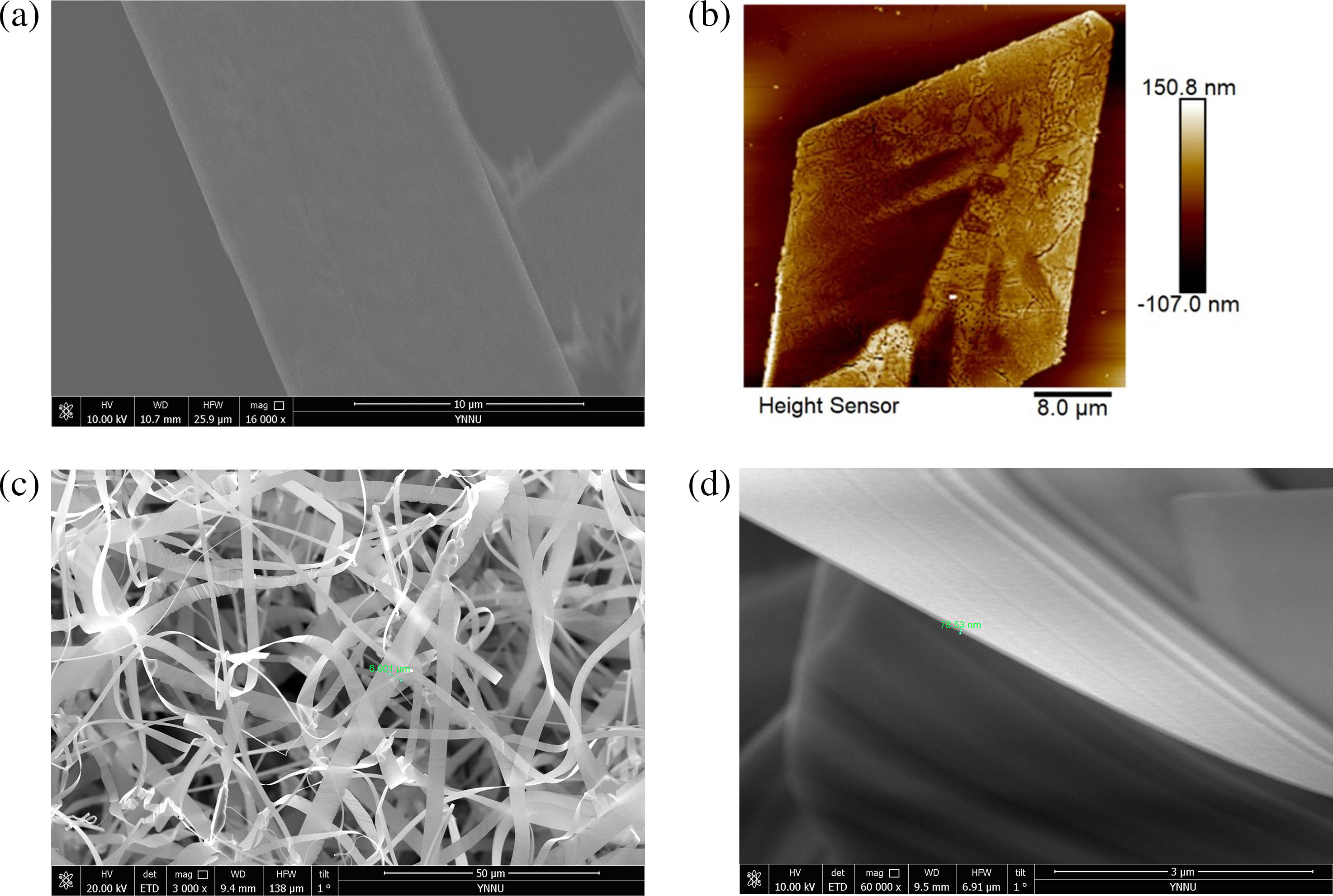
    Fig. 1. SEM and AFM images of FAPbBr3 NS and CdS NBs. (a) SEM image of FAPbBr3 nanosheet; (b) AFM image of a single FAPbBr3 nanosheet; (c) SEM image of CdS NBs; (d) cross section of CdS NBs.
    XRD patterns of the samples: (a) CdS NBs; (b) FAPbBr3 NSs.
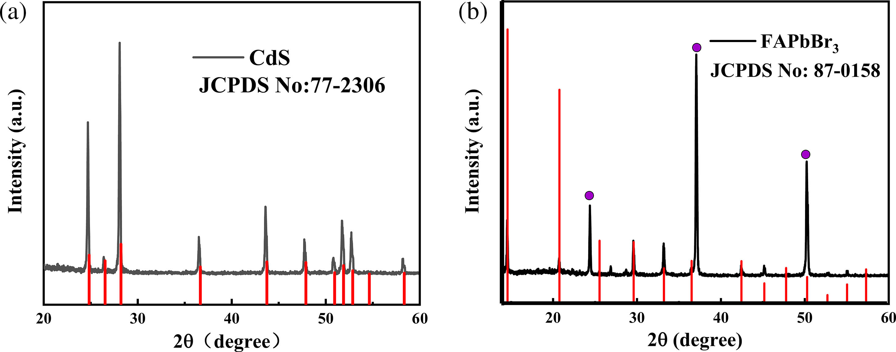
    Fig. 2. XRD patterns of the samples: (a) CdS NBs; (b) FAPbBr3 NSs.
    Spectral response of FAPbBr3 NS/CdS NB hybrid structure. (a) UV-Vis absorption spectra; (b) (αhν)2 versus photon energy curve of FAPbBr3 NS; (c) and (d) spectral response of FAPbBr3 NS device and FAPbBr3 NS/CdS NB hybrid structures at a bias voltage of 5 V.
    Fig. 3. Spectral response of FAPbBr3 NS/CdS NB hybrid structure. (a) UV-Vis absorption spectra; (b) (αhν)2 versus photon energy curve of FAPbBr3 NS; (c) and (d) spectral response of FAPbBr3 NS device and FAPbBr3 NS/CdS NB hybrid structures at a bias voltage of 5 V.
    (a) Schematic diagram of single FAPbBr3 NS and (b) FAPbBr3 NS/CdS NB hybrid structure device; (c), (d) SEM images of single FAPbBr3 NS and FAPbBr3 NS/CdS NB hybrid structure device, respectively; (e), (f) I-V curves of a single FAPbBr3 NS device and FAPbBr3 NS/CdS NB device under 490 nm light irradiation, respectively.
    Fig. 4. (a) Schematic diagram of single FAPbBr3 NS and (b) FAPbBr3 NS/CdS NB hybrid structure device; (c), (d) SEM images of single FAPbBr3 NS and FAPbBr3 NS/CdS NB hybrid structure device, respectively; (e), (f) I-V curves of a single FAPbBr3 NS device and FAPbBr3 NS/CdS NB device under 490 nm light irradiation, respectively.
    Performance of FAPbBr3 NS/CdS NB photodetector. (a) and (b) I-V curves; (c) and (d) photocurrent versus optical power density; (e), (f) EQE and (g), (h) D* of single FAPbBr3 NS device and CdS NB/FAPbBr3 NS hybrid devices with increased light intensity under 490 nm laser at a bias voltage of 5 V.
    Fig. 5. Performance of FAPbBr3 NS/CdS NB photodetector. (a) and (b) I-V curves; (c) and (d) photocurrent versus optical power density; (e), (f) EQE and (g), (h) D* of single FAPbBr3 NS device and CdS NB/FAPbBr3 NS hybrid devices with increased light intensity under 490 nm laser at a bias voltage of 5 V.
    I–t characteristic curve of FAPbBr3 NS/CdS NB photodetector. (a) Rising and falling edges of a single cycle with 5 V voltage offset; (b) photocurrent variation with time of CdS NB/FAPbBr3 NS hybrid device; (c) photocurrent of the device.
    Fig. 6. I–t characteristic curve of FAPbBr3 NS/CdS NB photodetector. (a) Rising and falling edges of a single cycle with 5 V voltage offset; (b) photocurrent variation with time of CdS NB/FAPbBr3 NS hybrid device; (c) photocurrent of the device.
    (a) Simulated electric field density distribution of different structures under light irradiation at 490 nm and (b) electric field distribution of a single FAPbBr3; (c) and (d) electric field distributions of the FAPbBr3/CdS hybrid device.
    Fig. 7. (a) Simulated electric field density distribution of different structures under light irradiation at 490 nm and (b) electric field distribution of a single FAPbBr3; (c) and (d) electric field distributions of the FAPbBr3/CdS hybrid device.
    Device StructureOn/Off RatioResponsivity (A/W)EQE (%)D* (Jones)Rise/Decay TimeRef.
    2D (OA) 2FAn-1PbnBr3n+1320.25/1.45 ms[30]
    FAPbBr3 microcrystal4 × 1043.87 × 10140.67/0.75 ms[31]
    FAPbBr3 QDs/graphene1.15 × 1053.42 × 10758/60 ms[32]
    MA0.7FA0.3PbBr31050.514.0 × 10126.7/2.5 ms[33]
    FAPbI31.4 × 1033.276301.35 × 10120.35/0.54 ms[34]
    a-FAPbI310511.465.4/10.9 ms[13]
    FAPbBr3 NS/CdS NB5.92 × 10457121.452 × 1041.8 × 101441.4/57.7 msThis work
    Table 1. Comparison of the Proposed Photodetector with Other Reported Devices in Terms of Photoresponse Parameters
    Yao Liu, Lei Liu, Ruifeng Zhang, Weiye Yang, Yingkai Liu. High-response formamidine bromide lead hybrid cadmium sulfide photodetector[J]. Chinese Optics Letters, 2024, 22(2): 022502
    Download Citation