【AIGC One Sentence Reading】:A hybrid photodetector combining FAPbBr3 nanosheets and CdS nanobelts offers enhanced stability and performance, with a high response under 490 nm light and maintained photocurrent after 60 days of air exposure.
【AIGC Short Abstract】:In this study, a hybrid photodetector combining formamidinium lead bromide nanosheets with cadmium sulfide nanobelts exhibits enhanced stability and performance. The device achieves a remarkable response of 5712 A/W under 490 nm illumination, significantly surpassing the performance of the pure FAPbBr3 photodetector. The hybrid device maintains nearly 80.25% of its initial photocurrent after 60 days in air, highlighting its durability. This innovation opens new avenues for highly stable, rapid-response photodetectors.
Note: This section is automatically generated by AI . The website and platform operators shall not be liable for any commercial or legal consequences arising from your use of AI generated content on this website. Please be aware of this.
Abstract
Organic–inorganic hybrid perovskite formamidinium lead bromide nanosheet (FAPbBr3 NS) is regarded as a superior substance used to construct optoelectronic devices. However, its uncontrollable stability seriously affects its application in the field of photodetectors. In this paper, FAPbBr3 is combined with cadmium sulfide nanobelt (CdS NB) to construct a hybrid device that greatly improves the stability and performance of the photodetector. The response of the FAPbBr3 NS/CdS NB detector under 490 nm light illumination reaches 5712 A/W, while the response of the FAPbBr3 photodetector under equivalent conditions is only 25.45 A/W. The photocurrent of the FAPbBr3 NS/CdS NB photodetector is nearly 80.25% of the initial device after exposure to air for 60 days. The difference in electric field distribution between the single material device and the composite device is simulated by the finite-difference time-domain method. It shows the advantages of composite devices in photoconductive gain and directly promotes the hybrid device performance. This paper presents a new possibility for high stability, fast response photodetectors.1. Introduction
During the last decade, organic–inorganic hybrid chalcogenides have attracted intense attention as a consequence of their excellent optical properties, such as high optical absorption coefficients[1–3], carrier mobility, and long carrier diffusion[4,5]. These intrinsic features make them attractive for various applications, including photodetectors[6–8], solar cells[9], LEDs[10–12], and laser devices[12]. Compared with and , has pure green light emission and better chemical stability[2]. Recently, Li et al. used as high-performance photodetector[13]. The Zeng group has fabricated perovskite nanoparticles by an ion exchange mediated self-assembly method[14]. Research revealed that is a potential candidate for optoelectronic devices due to its longer carrier lifetime and diffusion lengths[15].
Cadmium sulfide (CdS) is one of the most excellent II–VI semiconductors with a direct bandgap (), thermal and chemical stability, a high refractive index, and a relatively low work function. The design and manufacture of CdS photodetectors based on nanowires[16], nanoribbons[17], and nanorods[18] have been investigated. In past years, researchers employed inorganic CdS, CdSe as well as to mediate optoelectronic performance of organic perovskites[19,20]. Compared with other inorganic materials, CdS has higher responsivity and a larger on/off ratio, and the photoelectric performance of CdS hybrid devices is better than that of CdSe and other materials[21–23]. Moreover, there are few reports on hybrid devices with formamidinium lead bromide nanosheet ( NS). Therefore, we choose CdS to mediate organic–inorganic hybrid perovskites.
In this work, we prepared NS by the solution method and CdS nanobelt (NB) by PVD. NS/CdS NB detector was successfully constructed, and its optoelectronic property was measured. It was found that it exhibits an outstanding responsivity of 5712 A/W and on/off ratio of , originating from the high photoelectric conversion efficiency of NS. Exposure to the atmosphere with 50% humidity and 25°C, it was found that the undergone optimization perovskite device demonstrated a sustained performance retention of 80.25% over a period of 60 days.
Sign up for Chinese Optics Letters TOC. Get the latest issue of Chinese Optics Letters delivered right to you!Sign up now
2. Experimental Section
2.1. Preparation of FAPbBr3 NS and CdS NB
0.5 mmol (62.5 mg) FABr and 0.5 mmol (183.4 mg) was added to 1 mL mixed solution of dimethyl sulfoxide (DMSO) and N,N-dimethylformamide (DMF) with the ratio of 7:3 (DMSO to DMF) and stirred for 6 h at 60°C. After that, the precursor solution was filtered by a 0.24 µm polytetrafluoroethylene needle filter and 2.5 µL of solution was extracted, added dropwise to substrate and then dried on a heating table at 40°C for 24 h. FABr and were purchased from Polymer Light Technology Corp., Xi’an.
The synthesis of CdS NBs was conducted using a tube furnace containing a quartz tube with a diameter of 25 mm. Initially, a ceramic container with an adequate quantity of CdS powder was positioned at the center of the quartz tube. Subsequently, silicon (Si) wafers that had been subjected to a cleaning process were coated with gold particles by a sputtering technique for a duration of 100 s. These coated wafers were then positioned at both the upstream and downstream ends of the quartz tube. Subsequently, the adequately filled quartz tubes were moved to a tube furnace, wherein the temperature was initially elevated to 300°C for a duration of 30 min. Following this, the quartz tubes were kept at this temperature for 10 min and then the temperature was gradually increased to 835°C at a rate of 8°C/min and sustained at this level for 60 min. In the entire operation, the quartz tube was filled with argon gas, which contained 5% (volume fraction) hydrogen () at a flow rate of 15 standard cubic centimeters per minute (sccm).
2.2. Fabrication of FAPbBr3 NS/CdS NB photodetector
First, Ti/Au electrodes (5/45 nm) were fabricated on substrates by electron beam evaporation, and then the grown nanosheets were transferred to the electrodes by the PDMS-assisted dry method. Therewith, CdS NB was dispersed onto a clean substrate, adhesive CdS NB with PDMS film, and transferred to NS to complete the device preparation; finally, the device underwent annealing at a temperature of 100°C for a duration of 10 min.
3. Results and Discussion
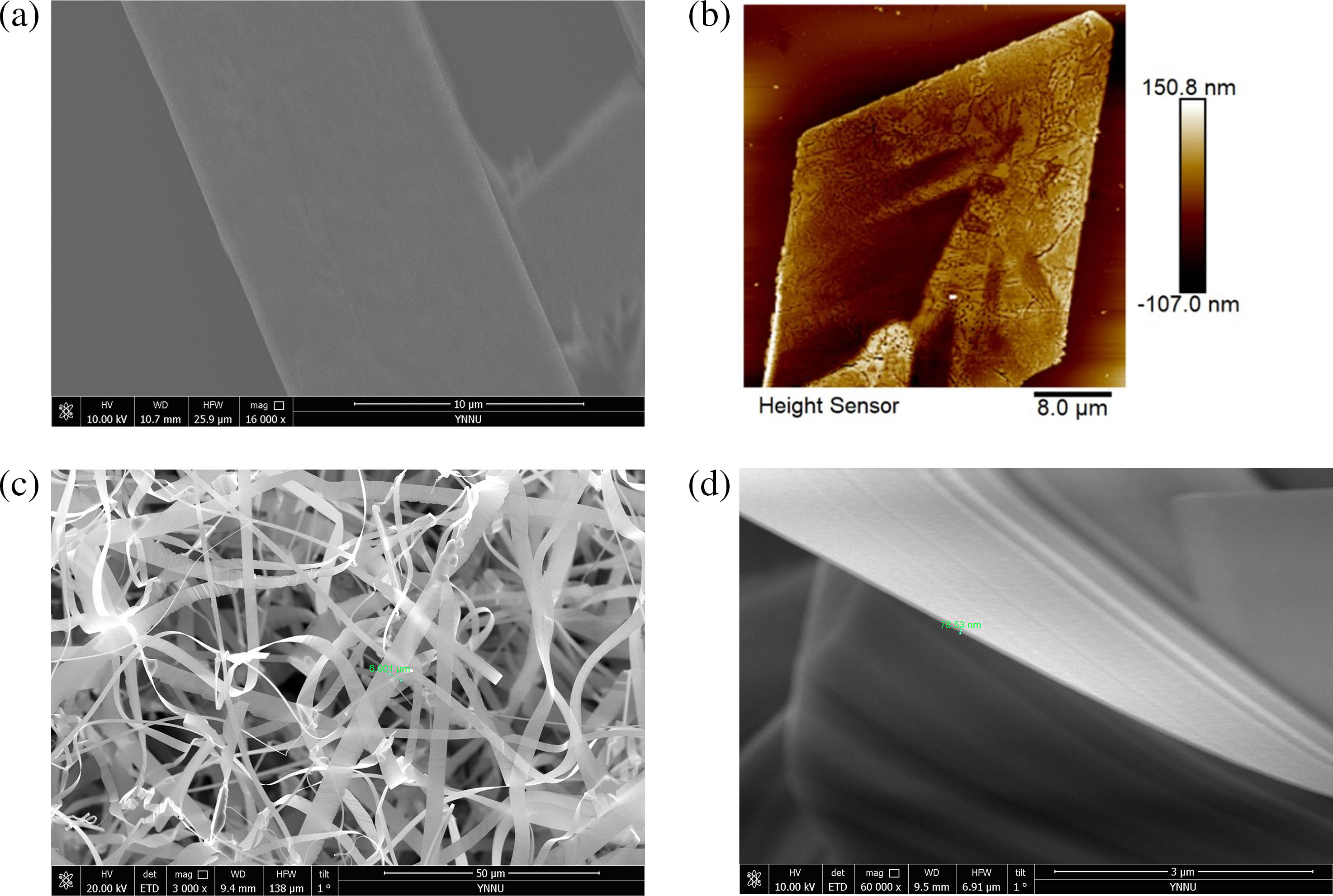
A scanning electron microscope (SEM) image of a single NS is shown in Fig. 1(a). The NSs form an asymmetric polygon. Figure 1(b) shows an AFM image of with a thickness of 150 nm. Figures 1(c) and 1(d) display SEM images of CdS NBs. It can be seen that the width of CdS NBs is about 10 µm and the thickness is about 70 nm. X-ray diffraction (XRD) was employed to reveal the crystal structures of NS and CdS NBs, as depicted in Fig. 2. The diffraction peaks of CdS NBs are presented in Fig. 2(a). The peaks are situated at 24.83°, 26.53°, 28.21°, 36.66°, 43.73°, 47.89°, 50.94°, 51.88°, 52.86°, and 58.35° corresponding to (100), (002), (101), (102), (110) (103), (200), (112), (201), (004), and (104) crystal planes, respectively, in good agreement with the standard card (standard card JCPDS No. 77-2306). This suggests that the prepared CdS NBs in this study exhibit a high degree of crystallinity and possess a pure crystalline phase. The XRD pattern of NS is illustrated in Fig. 2(b). The peaks at 14.52°, 20.72°, 29.58°, 33.18°, 42.45°, and 45.26 ° match with (100), (110), (200), (211), (220), and (300) crystal planes (standard card JCPDS No. 87-0158). These results are also in agreement with those reported elsewhere[24,25]. The peaks at 24.39°, 39.06°, and 50.21° marked by purple dots correspond to the (011), (212), and (211) crystal planes of (standard card JCPDS No. 82-1566), as shown in Fig. 2(b); the preparation of NSs is on the Si substrate with 500 nm-thick layer.

Figure 1.SEM and AFM images of FAPbBr3 NS and CdS NBs. (a) SEM image of FAPbBr3 nanosheet; (b) AFM image of a single FAPbBr3 nanosheet; (c) SEM image of CdS NBs; (d) cross section of CdS NBs.
Figure 2.XRD patterns of the samples: (a) CdS NBs; (b) FAPbBr3 NSs.
The spectral response of the CdS heterostructure was investigated. Figure 3(a) shows UV-Vis absorption spectra of and CdS hybrid structures in the range of 300–800 nm. According to Tauc’s[26] diagram, it is represented by the following equation: where is the absorption coefficient, is Planck’s constant, is the frequency of light, is the proportionality constant, and is the bandgap. is one-half for the direct bandgap. The calculated bandgap of is 2.24 eV in Fig. 3(b). The highest absorption of the hybrid NS/CdS NB structure is located at 490 nm, whereas the hybrid structure exhibits a much improved absorption rate in the range of 300 to 530 nm in Fig. 3(a). It was found that there are two descending platforms in the absorption spectrum of . The first peak at 350 nm corresponds to the absorption of due to the extra in the preparation of for UV-Vis absorption measurement. The second peak at 530 nm originated from . Therefore, two descending platforms are formed in the absorption spectrum of . This phenomenon may be attributed to the coupled light absorption of CdS NBs and NS. The enhanced absorption is advantageous for the performance of NSs/CdS NBs hybrid devices. To better understand the response of and NS/CdS NB hybrid structures, the responsive curves of the two structures were measured in the range of 300–600 nm, respectively, as displayed in Figs. 3(c) and 3(d). It can be seen that the NS/CdS NB hybrid structure has a broad responsive band at the wavelength of 400–500 nm, with two peaks located at 400 and 490 nm.
Figure 3.Spectral response of FAPbBr3 NS/CdS NB hybrid structure. (a) UV-Vis absorption spectra; (b) (αhν)2 versus photon energy curve of FAPbBr3 NS; (c) and (d) spectral response of FAPbBr3 NS device and FAPbBr3 NS/CdS NB hybrid structures at a bias voltage of 5 V.
Figure 4.(a) Schematic diagram of single FAPbBr3 NS and (b) FAPbBr3 NS/CdS NB hybrid structure device; (c), (d) SEM images of single FAPbBr3 NS and FAPbBr3 NS/CdS NB hybrid structure device, respectively; (e), (f) I-V curves of a single FAPbBr3 NS device and FAPbBr3 NS/CdS NB device under 490 nm light irradiation, respectively.
Figures 4(a) and 4(b) show the device schematic diagram of the NS and NS/CdS NB device. Figures 4(c) and 4(d) are their corresponding SEM images. Figure 4(c) shows the effective area of devices is . It is clearly seen that CdS is covered on , and the effective area of the device is in Fig. 4(d). Their photoelectric properties will be systematically investigated at 490 nm and a power density of , as described in Figs. 4(e) and 4(f). The photocurrent and dark current of the hybrid NS/CdS NB device ( NS one) at a bias voltage of 5 V are 1.19 µA (2.01 nA) and 20.1 pA (22.64 pA) with an on/off ratio of (). The on/off ratio of the front is times as large as that of the latter. Figures 5(a) and 5(b) show I-V curves of the and NS/CdS NB devices at 490 nm under light irradiation with different power densities. The observed trend indicates that there is a positive correlation between the power density and photocurrent, indicating that the effectiveness of the photocarriers is directly proportional to the quantity of photons absorbed. The photocurrent versus optical power density curve is plotted and fitted as , where , , and are the photocurrent, proportionality constant, and incident light intensity, respectively. The exponent determines the photocurrent response of the device toward light intensity. The fitted values of are 0.889 and 0.959 for and NS/CdS NB devices, respectively, as illustrated in Figs. 5(c) and 5(d). They are slightly less than the ideal value of 1, revealing that NS and NS/CdS NB devices have excellent optical exchange capability and have fewer defects. To further compare the performance of NS and NS/CdS NB detectors, the responsivity (), external quantum efficiency (EQE), and specific detectivity () are evaluated by the following formula[7,8,27–29]: where is the photocurrent, is the dark current, is the incident light intensity, is the effective illuminance area, is the electron charge, is Planck’s constant, and and are the velocity and wavelength of the incident light, respectively.
Figure 5.Performance of FAPbBr3 NS/CdS NB photodetector. (a) and (b) I-V curves; (c) and (d) photocurrent versus optical power density; (e), (f) EQE and (g), (h) D* of single FAPbBr3 NS device and CdS NB/FAPbBr3 NS hybrid devices with increased light intensity under 490 nm laser at a bias voltage of 5 V.
Based on the above equations, we obtained , EQE, and of and NS/CdS NB detectors. The relationships of , EQE, and versus power density are depicted in Figs. 5(e), 5(f), 5(g), and 5(h). It is exhibited that the maximum , EQE, and for the single photodetector are 25.45 A/W, 64.5%, and Jones. The maximum , EQE, and of the NS/CdS NB hybrid detector are , , and Jones, at least being 2 orders of magnitude higher than that of the single NS one.
One of the most important metrics for describing the photodetector is the response time. The rising and falling edges of the device are depicted in Fig. 6(a), in which the rise time (10% to 90% of the maximum current) and the decay time (90% to 10% of the maximum current) are calculated to be 41.42 and 57.7 ms, respectively. Figure 6(b) shows I-t curves under an illumination of 490 nm with continuous on and off at bias voltages of 5 V. This told us about the reproducible and reversible photodetective behavior of the NS/CdS NB device. The photocurrent of the device was 80.25% of that of the initial period in Fig. 6(c), whereas the rise time/decay time is 42.18/58.04 ms after being stored in air for 60 days. The sensitivity of the device to light shows a weak attenuation.
Figure 6.I–t characteristic curve of FAPbBr3 NS/CdS NB photodetector. (a) Rising and falling edges of a single cycle with 5 V voltage offset; (b) photocurrent variation with time of CdS NB/FAPbBr3 NS hybrid device; (c) photocurrent of the device.
To provide a better comparison, we summarize the photoelectric metrics of FA-based photodetector devices, as listed in Table 1. The device exhibited a notable enhancement in its photovoltaic performance, with some critical metrics experiencing an increase of at least 1 order of magnitude. Meanwhile, the NS/CdS NB hybrid device is competitive with most FA-based photodetector devices, due to their better optoelectronic performance.
| Device Structure | On/Off Ratio | Responsivity (A/W) | EQE (%) | D* (Jones) | Rise/Decay Time | Ref. |
|---|
| 2D (OA) 2FAn-1PbnBr3n+1 | – | 32 | – | – | 0.25/1.45 ms | [30] |
| FAPbBr3 microcrystal | – | 4 × 10⁴ | – | 3.87 × 10¹⁴ | 0.67/0.75 ms | [31] |
| FAPbBr3 QDs/graphene | – | 1.15 × 10⁵ | 3.42 × 10⁷ | – | 58/60 ms | [32] |
| MA0.7FA0.3PbBr3 | 105 | 0.51 | | 4.0 × 10¹² | 6.7/2.5 ms | [33] |
| FAPbI3 | 1.4 × 10³ | 3.27 | 630 | 1.35 × 10¹² | 0.35/0.54 ms | [34] |
| a-FAPbI3 | 105 | 11.46 | – | – | 5.4/10.9 ms | [13] |
| FAPbBr3 NS/CdS NB | 5.92 × 10⁴ | 5712 | 1.452 × 10⁴ | 1.8 × 10¹⁴ | 41.4/57.7 ms | This work |
Table 1. Comparison of the Proposed Photodetector with Other Reported Devices in Terms of Photoresponse Parameters
As the incident wavelength is larger than 530 nm, the responsivity of the device rapidly decreases, which is closely associated with the energy of the photon radiated. For the experiment, there will be a transition from impurities to the band. The energy of the photons absorbed by the electrons in the valence band of the jumped to the conduction band, as the wavelength of the incident light is less than 530 nm. Under the effect of the internal electric field, the electrons and holes have different quasi-Fermi energy levels due to the generated electron–hole pairs by light. The hole concentration does not change, so the net free electron concentration increases[35]. To measure the photoelectric characteristic curve, the curve moves to the left. In order to elucidate the effect of geometry on optical properties and the optical response of the heterojunction devices, the distributions of electric field density in perovskite materials (150 nm in thickness)/CdS nanobelt (70 nm in thickness) heterostructures were estimated by numerical calculations using the FDTD method. In order to streamline the model, the dimensions of the perovskite were established as 5000 nm in length and 500 nm in breadth. In the data depicted in Fig. 7(a), the perovskite material exhibits localized regions of intense electric fields (commonly referred to as hot spots) inside its surface region upon exposure to 490 nm light. This observation implies that the perovskite has the capability to effectively restrict incident visible light. Importantly, this photo-limiting effect can be further enhanced by transferring[36] from the CdS belt to the surface of the perovskite. The augmentation in electric field intensity in the surface region of the nanostructure is readily apparent, leading to an increased efficacy in optical coupling and capture. The observed behavior may be comprehended due to the light-trapping effect often arising from the reflections occurring at the perimeters of the perovskite material. It is noteworthy that the optical characteristics of the aforementioned structures exhibit a high degree of consistency. In contrast to the single perovskite structure, it exhibits a shallow field penetration depth, resulting in a significantly restricted optical coupling capacity [Fig. 7(c)]. The theoretical simulation results are in good agreement with the optical response performance of the device. Figure 5(b) shows I-V curves of the perovskite/CdS NB heterostructure and the current-voltage curves of a single perovskite/CdS heterojunction under the same lighting irradiation. It is noted that the increase in photocurrent and stronger photovoltaic behavior may be due to the improved absorption of light by heterojunction with a larger area. Furthermore, the individual perovskite has inferior photoelectric characteristics to its limited light absorption capability. Based on the aforementioned study, it can be concluded that the perovskite/CdS heterojunction possesses a superior option for attaining photodetectors with high-performance capabilities.
Figure 7.(a) Simulated electric field density distribution of different structures under light irradiation at 490 nm and (b) electric field distribution of a single FAPbBr3; (c) and (d) electric field distributions of the FAPbBr3/CdS hybrid device.
4. Conclusion
We have achieved the preparation of optoelectronic devices by transfer. The NS/CdS NB heterojunction photodetector exhibits high response in the range of 400–530 nm. It was stored in air for 60 days and still had 80.25% of its original achievement. The optical responsivity, external quantum efficiency, and detection rate were , , and Jones, respectively, when the optical power was (at 490 nm). The response time of the photodetector in the 490 nm spectral range is short (). Based on the photoelectric response mechanism, the photoelectric performance of the device is related to the efficiency of light capture and coupling, and the performance of the detector can be further improved by optimizing this method. The transfer of to different substrates makes it an excellent candidate for different optoelectronic devices.
References
[1] F. Hao, C. C. Stoumpos, D. H. Cao et al. Lead-free solid-state organic-inorganic halide perovskite solar cells. Nat. Photonics, 8, 489(2014).
[2] K. M. Boopathi, R. Mohan, T.-Y. Huang et al. Synergistic improvements in stability and performance of lead iodide perovskite solar cells incorporating salt additives. J. Mater. Chem C, 4, 1591(2016).
[3] W. Shangguan, C. X. Yan, J. M. Cai. Quasi-planar tetracoordiante carbon networks with tunable electronic properties combined with ultra-high carrier mobility and optical absorption coefficient: two-dimensional Be2C. Appl. Surf. Sci., 604, 154644(2022).
[4] H. S. Kim, C. R. Lee, J. H. Im et al. Lead iodide perovskite sensitized all-solid-state submicron thin film mesoscopic solar cell with efficiency exceeding 9%. Sci. Rep., 2, 591(2012).
[5] Q. F. Dong, Y. J. Fang, Y. C. Shao et al. Electron-hole diffusion lengths < 175 µm in solution-grown CH3NH3PbI3 single crystals. Science, 347, 967(2015).
[6] S. A. Veldhuis, P. P. Boix, N. Yantara et al. Perovskite materials for light-emitting diodes and lasers. Adv. Mater., 28, 6804(2016).
[7] X. Liu, L. L. Gu, Q. P. Zhang et al. All-printable band-edge modulated ZnO nanowire photodetectors with ultra-high detectivity. Nat. Commun., 5, 4007(2014).
[8] S. X. Li, H. Xia, X. C. Sun et al. Curved photodetectors based on perovskite microwire arrays via in situ conformal nanoimprinting. Adv. Funct. Mater., 32, 2202277(2022).
[9] D. P. Mcmeekin, G. Sadoughi, W. Rehman et al. A mixed-cation lead mixed-halide perovskite absorber for tandem solar cells. Science, 351, 151(2016).
[10] Z. G. Xiao, R. A. Kerner, L. F. Zhao et al. Efficient perovskite light-emitting diodes featuring nanometre-sized crystallites. Nat. Photonics, 11, 108(2017).
[11] Q. Shan, J. Li, J. Song et al. All-inorganic quantum-dot light-emitting diodes based on perovskite emitters with low turn-on voltage and high humidity stability. J. Mater. Chem. C, 5, 4565(2017).
[12] L. Meng, E. P. Yao, Z. R. Hong et al. Pure formamidinium-based perovskite light-emitting diodes with high efficiency and low driving voltage. Adv. Mater., 29, 1603826(2017).
[13] S. G. Li, S. C. Tong, J. L. Yang et al. High-performance formamidinium-based perovskite photodetectors fabricated via doctor-blading deposition in ambient condition. Org. Electron., 47, 102(2017).
[14] D. J. Yu, F. Cao, Y. J. Gao et al. Room-temperature ion-exchange-mediated self-assembly toward formamidinium perovskite nanoplates with finely tunable, ultrapure green emissions for achieving Rec. 2020 displays. Adv. Funct. Mater., 28, 1800248(2018).
[15] A. A. Zhumekenov, M. I. Saidaminov, M. A. Haque et al. Formamidinium lead halide perovskite crystals with unprecedented long carrier dynamics and diffusion length. ACS Energy Lett., 1, 32(2016).
[16] T. Y. Wei, C. T. Huang, B. J. Hansen et al. Large enhancement in photon detection sensitivity via Schottky-gated CdS nanowire nanosensors. Appl. Phys. Lett., 96, 013508(2010).
[17] Y. Ye, L. Dai, X. N. Wen et al. High-performance single CdS nanobelt metal-semiconductor field-effect transistor-based photodetectors. ACS Appl. Mater. Interf., 2, 2724(2010).
[18] J. S. Jie, W. J. Zhang, Y. Jiang et al. Photoconductive characteristics of single-crystal CdS nanoribbons. Nano Lett., 6, 1887(2006).
[19] W. K. Bae, L. A. Padilha, Y. S. Park et al. Controlled alloying of the core-shell interface in CdSe/CdS quantum dots for suppression of auger recombination. ACS Nano, 7, 3411(2013).
[20] L. D. Li, Z. Lou, H. R. Chen et al. Stretchable SnO2-CdS interlaced-nanowire film ultraviolet photodetectors. Sci. China-Mater., 62, 1139(2019).
[21] B. H. Liu, M. K. Li, W. Fu et al. High-performance self-driven ultraviolet photodetector based on SnO2 p-n homojunction. Opt. Mater., 129, 112571(2022).
[22] J. Q. Huang, Q. H. Tan, Z. J. Zhang et al. Photoconductive properties of Er-CdSe nanobelt detectors. J. Mater. Sci., 54, 560(2019).
[23] Y. Ye, L. Dai, X. N. Wen et al. High-performance single CdS nanobelt metal-semiconductor field-effect transistor-based photodetectors. ACS Appl. Mater. Interfaces, 2, 2724(2010).
[24] V. K. Sharma, R. Mukhopadhyay, A. Mohanty et al. Contrasting behaviors of FA and MA cations in APbBr3. J. Phys. Chem. Lett., 11, 9669(2020).
[25] Y. H. Kim, C. Wolf, Y. T. Kim et al. Highly efficient light-emitting diodes of colloidal metal–halide perovskite nanocrystals beyond quantum size. ACS Nano, 11, 6586(2017).
[26] J. Zhang, X. K. Yang, H. Deng et al. Low-dimensional halide perovskites and their advanced optoelectronic applications. Nano-Micro Lett., 9, 26(2017).
[27] W. Zheng, F. Huang, R. S. Zheng et al. Low-dimensional structure vacuum-ultraviolet-sensitive (λ < 200 nm) photodetector with fast-response speed based on high-quality AlN micro/nanowire. Adv. Mater., 27, 3921(2015).
[28] Z. P. Lian, Q. F. Yan, Q. R. Lv et al. High-performance planar-type photodetector on (100) facet of MAPbI3 single crystal. Sci. Rep., 5, 16563(2015).
[29] B. Nafradi. Comment on ‘Superior photodetectors based on all-inorganic perovskite CsPbl3 nanorods with ultrafast response and high stability. ACS Nano, 12, 10570(2018).
[30] D. J. Yu, F. Cao, Y. L. Shen et al. Dimensionality and interface engineering of 2D homologous perovskites for boosted charge-carrier transport and photodetection performances. J. Phys. Chem. Lett., 8, 2565(2017).
[31] F. Y. Zhang, B. Yang, K. B. Zheng et al. Formamidinium lead bromide (FAPbBr3) perovskite microcrystals for sensitive and fast photodetectors. Nano-Micro Lett., 10, 8(2018).
[32] R. Pan, H. Y. Li, J. Wang et al. High-responsivity photodetectors based on formamidinium lead halide perovskite quantum dot-graphene hybrid. Part. Part. Syst. Charact., 35, 1700304(2018).
[33] H. Zhou, Z. Song, C. Wang et al. Double coating for the enhancement of the performance in a MA0.7FA0.3PbBr3 photodetector. ACS Photonics, 5, 2100(2018).
[34] D. J. Yu, F. Cao, Y. Gu et al. Broadband and sensitive two-dimensional halide perovskite photodetector for full-spectrum underwater optical communication. Nano Res., 14, 1210(2021).
[35] M. M. Furchi, D. K. Polyushkin, A. Pospischil et al. Mechanisms of photoconductivity in atomically thin MoS2. Nano Lett., 14, 6165(2014).
[36] L. Y. Cao, P. Y. Fan, A. P. Vasudev et al. Semiconductor nanowire optical antenna solar absorbers. Nano Lett., 10, 439(2010).
 AI Video Guide
  AI Picture Guide
 AI One Sentence