• Photonics Research
  • Vol. 9, Issue 4, 494 (2021)
Xiuli Li1、2, Linzhi Peng1、2, Zhi Liu1、2、*, Zhiqi Zhou3, Jun Zheng1、2, Chunlai Xue1、2, Yuhua Zuo1、2, Baile Chen3, and Buwen Cheng1、2、4
Author Affiliations
  • 1State Key Laboratory on Integrated Optoelectronics, Institute of Semiconductors, Chinese Academy of Sciences, Beijing 100083, China
  • 2Center of Materials Science and Optoelectronics Engineering, University of Chinese Academy of Sciences, Beijing 100049, China
  • 3School of Information Science and Technology, ShanghaiTech University, Shanghai 201210, China
  • 4Beijing Academy of Quantum Information Sciences, Beijing 100193, China
  • show less
    DOI: 10.1364/PRJ.413453 Cite this Article Set citation alerts
    Xiuli Li, Linzhi Peng, Zhi Liu, Zhiqi Zhou, Jun Zheng, Chunlai Xue, Yuhua Zuo, Baile Chen, Buwen Cheng. 30 GHz GeSn photodetector on SOI substrate for 2 µm wavelength application[J]. Photonics Research, 2021, 9(4): 494 Copy Citation Text show less
    (a) Cross-sectional transmission electron microscopy (TEM) image of the epitaxial material grown on the SOI substrate; the inset above is the selected-area diffraction pattern of the GeSn layer. (b) High-resolution TEM (HR-TEM) image of interface between epitaxial GeSn and Ge-buffer. (c) HR-TEM image of interface between epitaxial Ge-buffer and top-Si substrate. (d) The SIMS depth profile analysis of various elements in the as-grown sample. (e) X-ray diffraction reciprocal space map (XRD-RSM) around the asymmetric (−2-24) reflection of the material.
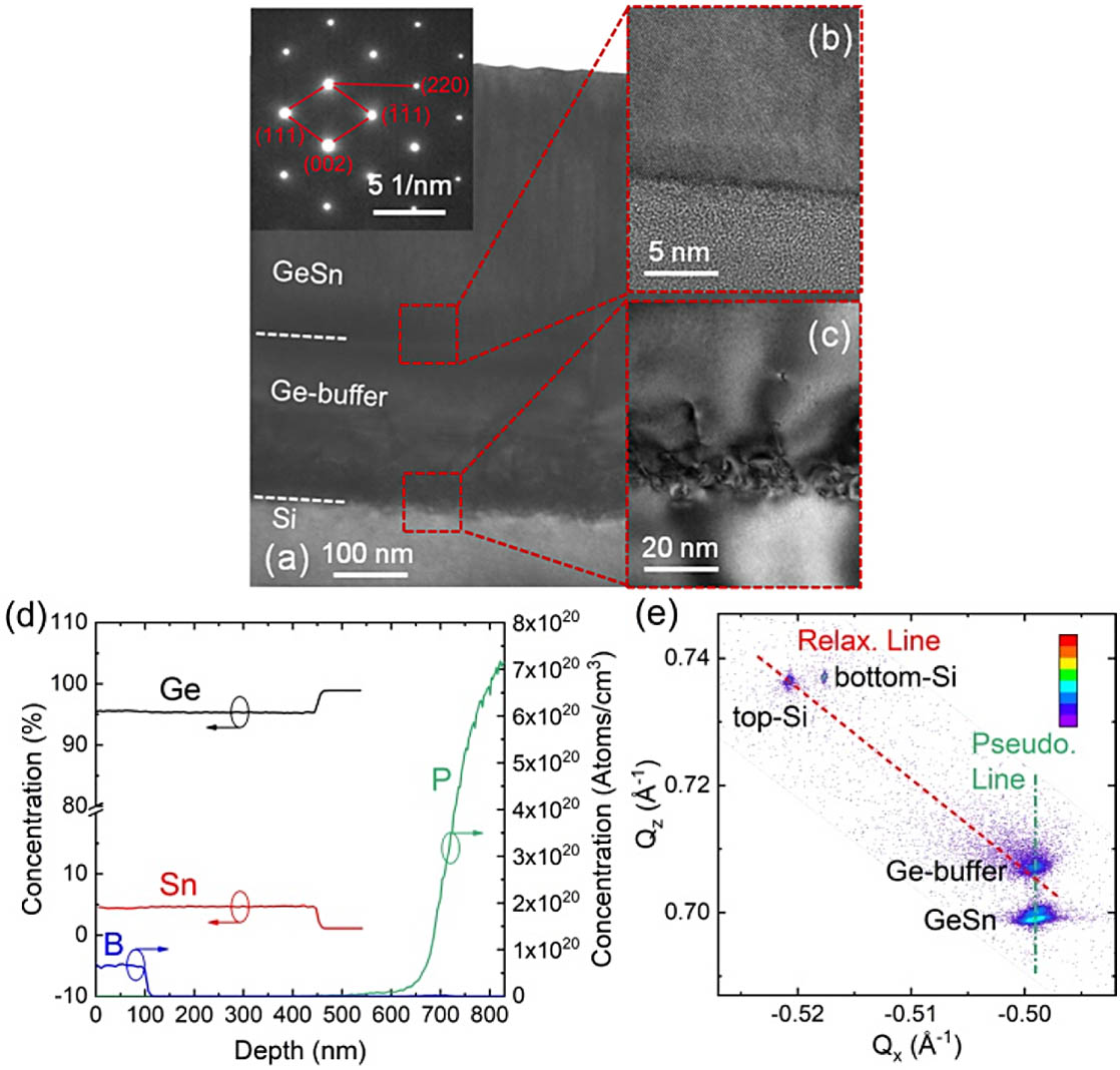
    Fig. 1. (a) Cross-sectional transmission electron microscopy (TEM) image of the epitaxial material grown on the SOI substrate; the inset above is the selected-area diffraction pattern of the GeSn layer. (b) High-resolution TEM (HR-TEM) image of interface between epitaxial GeSn and Ge-buffer. (c) HR-TEM image of interface between epitaxial Ge-buffer and top-Si substrate. (d) The SIMS depth profile analysis of various elements in the as-grown sample. (e) X-ray diffraction reciprocal space map (XRD-RSM) around the asymmetric (2-24) reflection of the material.
    (a) 3D structure schematic of the normally illuminated p-i-n Ge0.951Sn0.049 photodetector. (b) Top-view SEM image of the device with a 10 μm diameter mesa.
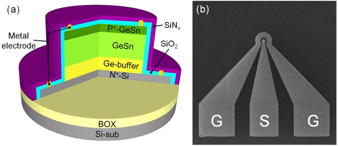
    Fig. 2. (a) 3D structure schematic of the normally illuminated p-i-n Ge0.951Sn0.049 photodetector. (b) Top-view SEM image of the device with a 10 μm diameter mesa.
    Typical I-V characteristics of the Ge0.951Sn0.049 photodetectors (D=10, 12, 15, 18, 20, 25, and 30 μm); the inset is the dark current densities of devices at −1 V versus 1/D.
    Fig. 3. Typical I-V characteristics of the Ge0.951Sn0.049 photodetectors (D=10, 12, 15, 18, 20, 25, and 30 μm); the inset is the dark current densities of devices at 1  V versus 1/D.
    (a) C-V characteristics of the Ge0.951Sn0.049 photodetectors with various diameters. (b) The capacitances of different devices at −3 V versus area.
    Fig. 4. (a) C-V characteristics of the Ge0.951Sn0.049 photodetectors with various diameters. (b) The capacitances of different devices at 3  V versus area.
    (a) I-V characteristics of the GeSn photodetector with a diameter of 10 μm with/without light incidence. (b) Spectrum response and optical responsivity of the Ge0.951Sn0.049 photodetector as functions of wavelength under zero-bias. Devices were measured by an FTIR optical spectrometer and lasers (two tunable lasers, one is located between 1260 nm and 1360 nm, and the other is located between 1500 nm and 1630 nm, and a laser at 2000 nm). The data are shown as a blue curve and a scatter plot, respectively.
    Fig. 5. (a) I-V characteristics of the GeSn photodetector with a diameter of 10 μm with/without light incidence. (b) Spectrum response and optical responsivity of the Ge0.951Sn0.049 photodetector as functions of wavelength under zero-bias. Devices were measured by an FTIR optical spectrometer and lasers (two tunable lasers, one is located between 1260 nm and 1360 nm, and the other is located between 1500 nm and 1630 nm, and a laser at 2000 nm). The data are shown as a blue curve and a scatter plot, respectively.
    Illustration of an optical heterodyne beat frequency measurement system.
    Fig. 6. Illustration of an optical heterodyne beat frequency measurement system.
    (a) Normalized frequency responses of the photodetectors with various diameters at 2 μm (D=10, 15, 20, 25, and 30 μm). (b) The theory RC-limited bandwidth, transit-time-limited bandwidth, and combined bandwidth of devices with different diameters.
    Fig. 7. (a) Normalized frequency responses of the photodetectors with various diameters at 2 μm (D=10, 15, 20, 25, and 30 μm). (b) The theory RC-limited bandwidth, transit-time-limited bandwidth, and combined bandwidth of devices with different diameters.
    Comparison of 3 dB bandwidth of high-speed photodetectors for 2 μm-wavelength light detection in different groups.
    Fig. 8. Comparison of 3 dB bandwidth of high-speed photodetectors for 2 μm-wavelength light detection in different groups.
    Layera (Å)a|| (Å)a0 (Å)ε|| (%)Sn (%)
    Ge5.65845.66705.66210.09
    GeSn5.72345.66755.7003−0.504.9
    Table 1. Summary of Lattice Constant, In-Plane Strain and Sn Concentration
    Device Diameter (μm)Dark Current Density (mA/cm2)Capacitance (fF)3-dB Bandwidth (GHz)
    10298.348.230
    15257.993.728
    20206.5148.717
    25192.5229.611
    30189.8311.78
    Table 2. Summary of Dark Current Density, Capacitance, and 3 dB Bandwidth of Devices with Different Diameters
    Xiuli Li, Linzhi Peng, Zhi Liu, Zhiqi Zhou, Jun Zheng, Chunlai Xue, Yuhua Zuo, Baile Chen, Buwen Cheng. 30 GHz GeSn photodetector on SOI substrate for 2 µm wavelength application[J]. Photonics Research, 2021, 9(4): 494
    Download Citation