
Xiuli Li, Linzhi Peng, Zhi Liu, Zhiqi Zhou, Jun Zheng, Chunlai Xue, Yuhua Zuo, Baile Chen, Buwen Cheng. 30 GHz GeSn photodetector on SOI substrate for 2 µ m wavelength application[J]. Photonics Research, 2021, 9(4): 494
- Photonics Research
- Vol. 9, Issue 4, 494 (2021)
Abstract
1. INTRODUCTION
At present, the industry standard wavelength range for telecommunication lies between 1.3 and 1.6 μm. However, the fiber-optic telecommunication system is gradually approaching its capacity limit since the exponential growth of internet data transmission, and the phenomenon of “capacity crunch” of the optical communication system may happen in the future [1,2]. This crisis can be temporarily alleviated by compressing the transmission data or adopting multiple parallel links communication. But the recent studies in hollow-core photonic bandgap fibers (HC-PBGFs) provide a more elegant solution; HC-PBGFs have demonstrated that the loss window can be extended from 1.55 to 2 μm, and the theoretical minimum loss is below 0.1 dB/km [3,4]. This loss is lower than the best conventional single-mode fiber (SMF) (0.1484 dB/km), and the proposed HC-PBGF–based communication system is compatible with silicon photonics, as the loss of silicon dioxide is low at 2 μm, and some strip and ridge waveguides with low transmission loss on silicon-on-insulator (SOI) platforms have been reported [5]. In addition, some optical components that can be used for 2 μm waveband optical communication have also made significant progress. For example, the optical gain window of thulium-doped fiber amplifiers (TDFAs) resides at around 1810–2050 nm, and it can be used as the equivalent to erbium-doped fiber amplifiers (EDFAs) in a 2 μm communication system [6,7]. The eight-channel wavelength division multiplexing system has a data transmission rate of 100 Gb/sat 2 μm, which consists of four internal direct modulation channels and four externally modulated channels [8]. Also, on the germanium-on-silicon (Ge-on-Si) platform, the all-optical modulator based on free carrier absorption working at around 55 MHz across the wavelength range of 2–3.2 μm [9], and a silicon-based high-speed Mach–Zehnder interferometer (MZI) modulator with a data transmission rate of 20 Gb/s at 2 μm have also been demonstrated [10]. Significant progress has also been made in 2 μm optical attenuators (VOAs) based on free carrier injection on the SOI platform and the Ge-on-Si platform [11]. These studies indicate that the 2 μm waveband has great potential as a candidate spectral window for future telecommunication systems.
The high-speed photodetector as an important optical component is also indispensable in optical communication systems. Because the bandgap of germanium-tin () alloys is adjustable and compatible with the existing complementary metal-oxide–semiconductor (CMOS) platform, some high-speed photodetectors based on GeSn binary alloys for 1.55 and 2 μm have been reported [12–15]. However, due to the large parasitic parameters, the bandwidth of the photodetectors working in the 2 μm band only achieves or less. Moreover, the differences in lattice constants between the Ge element and the Sn element and between Si and Sn are 14.7% and 19.5%, respectively. As the composition of Sn in the GeSn alloy increases, the compressive strain of the GeSn alloy will gradually increase. When the stress is unbearable, the strain will eventually be released in the form of dislocations. It will cause deterioration of material quality, and the electrical performance and high-speed performance of the device will also be seriously affected.
In this work, high-speed photodetectors on SOI substrates were designed and fabricated. The high-quality GeSn binary alloy was created using solid-source molecular beam epitaxy (MBE). A room temperature dark current density of is achieved when biased at . The parasitic capacitance and junction capacitance of the device are also extracted by the C–V curves. A remarkable optical responsivity of 14 mA/W is achieved at 2 μm. In addition, the frequency response characteristics of these photodetectors are studied. A 3 dB bandwidth up to 30 GHz is achieved at reverse bias, which is among the highest values reported in the literature for all group III–V and group IV photodetectors working in the 2 μm wavelength range. These results pave the way toward more promising feasibility of a new spectral window at the 2 μm wavelength.
Sign up for Photonics Research TOC. Get the latest issue of Photonics Research delivered right to you!Sign up now
2. MATERIAL GROWTH AND CHARACTERISTICS
The materials were grown using solid-source MBE on an SOI substrate, which contains a 220 nm thick Si top layer and a 2 μm thick buried oxide layer (BOX). Before the materials were created, the superficial Si layer went through phosphorus diffusion to form the -type contact layer. Afterward, a standard Radio Corporation of America (RCA) wet-chemical cleaning recipe was used to clean the substrate. Then, the wafer was loaded into the chamber for degassing at 300°C. Subsequently, the substrate was deoxidized at 850°C for 10 min. The complete layer sequence of nominally designed epitaxial layer includes a 200 nm thick Ge-buffer layer grown using a two-step growth process, composed of a 70 nm thick low temperature (LT-Ge) deposited at 300°C and a layer of 130 nm thick high temperature (HT-Ge) grown at 600°C. In order to reduce the lattice mismatch dislocations, the Ge-buffer underwent cyclic annealing from 600°C to 750°C after growth. A 350 nm thick GeSn alloy layer was deposited at 200°C, and a 100 nm thick -type boron-doped GeSn layer was grown at the same temperature to avoid segregation of Sn atoms in the GeSn layer.
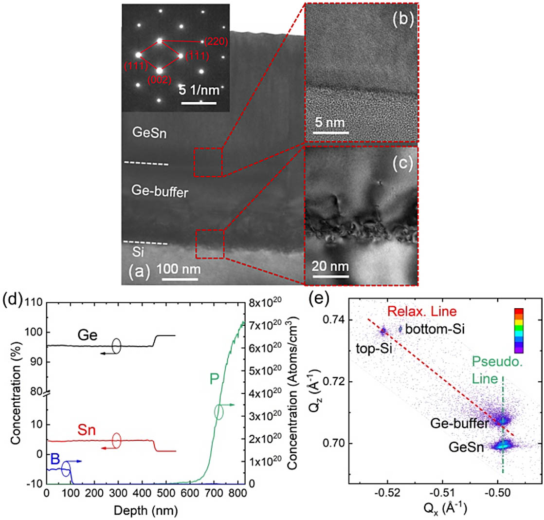
Figure 1.(a) Cross-sectional transmission electron microscopy (TEM) image of the epitaxial material grown on the SOI substrate; the inset above is the selected-area diffraction pattern of the GeSn layer. (b) High-resolution TEM (HR-TEM) image of interface between epitaxial GeSn and Ge-buffer. (c) HR-TEM image of interface between epitaxial Ge-buffer and top-Si substrate. (d) The SIMS depth profile analysis of various elements in the as-grown sample. (e) X-ray diffraction reciprocal space map (XRD-RSM) around the asymmetric (
3. DEVICE FABRICATION
![]()
Figure 2.(a) 3D structure schematic of the normally illuminated p-i-n
4. ELECTRICAL CHARACTERISTICS
![]()
Figure 3.Typical
![]()
Figure 4.(a)
5. PHOTOCURRENT AND SPECTRUM RESPONSIVITY
![]()
Figure 5.(a)
The spectral response of the photodetector was measured using a Nicolet 6700 Fourier transform infrared (FTIR) spectrometer, and a commercial InGaAs photodetector was used to calibrate spectrum responsivity. Figure 5(b) shows the spectral response of the photodetector under zero-bias. The scatter plot, which was measured by a 1260–1360 nm tunable laser, a 1500–1630 nm tunable laser, and a 2 μm laser at 0 V reverse-bias voltage, corresponds well to the spectrum response indicated by the blue curve. A resonance responsivity peak around is clearly observed, and the responsivities are 0.25 and 0.31 A/W at 1550 and 1625 nm wavelengths, respectively. Obviously, compared with Ge-on-Si photodetectors, the device in this work can significantly extend the detection wavelength. The optical response covers the O, E, S, C, L, and U telecommunication bands completely, and a new 2 μm communication window can also be implied.
6. FREQUENCY RESPONSES
![]()
Figure 6.Illustration of an optical heterodyne beat frequency measurement system.
![]()
Figure 7.(a) Normalized frequency responses of the photodetectors with various diameters at 2 μm (
The bandwidth of photodetector is mainly dominated by the carrier transit-time-limited bandwidth () and resistor capacitor (RC)-limited bandwidth () in the active region. and can be written as [31]
![]()
Figure 8.Comparison of 3 dB bandwidth of high-speed photodetectors for 2 μm-wavelength light detection in different groups.
7. CONCLUSIONS
In summary, a high-speed silicon-based photodetector is fabricated on SOI substrates for 2 μm wavelength light detection. A low dark current density of is achieved at . The parasitic capacitance and junction capacitance are extracted as 17.5 fF and , respectively. At bias voltages of , the optical responsivity of the photodetector is 14 mA/W at 2 μm. In addition, this GeSn photodetector achieved a 3 dB bandwidth as high as 30 GHz, which is among the highest values for 2 μm wavelength optical communications. And, the experimental values of the 3 dB bandwidth under different diameters are consistent with simulated results. The excellent high-speed performance of this device proves that Si-based GeSn photodetectors have great potential in the new 2 μm communication band, which can effectively increase the communication capacity in the future.
References
[10] W. Cao, D. Hagan, D. J. Thomson, M. Nedeljkovic, C. G. Littlejohns, A. Knights, S.-U. Alam, J. Wang, F. Gardes, W. Zhang, S. Liu, K. Li, M. S. Rouifed, G. Xin, W. Wang, H. Wang, G. T. Reed, G. Z. Mashanovich. High-speed silicon modulators for the 2 μm wavelength band. Optica, 5, 1055-1062(2018).

Set citation alerts for the article
Please enter your email address
© Copyright 2018-2021 | Chinese Laser Press. All Rights Reserved 沪ICP备15018463号-20