• Chinese Optics Letters
  • Vol. 16, Issue 5, 050007 (2018)
Mohammad Alavirad1、2, Anthony Olivieri2, Langis Roy3, and Pierre Berini2、4、5、*
Author Affiliations
  • 1Department of Electronics, Carleton University, 1125 Colonel By Drive, Ottawa, Ontario K1S 5B6, Canada
  • 2Centre for Research in Photonics, University of Ottawa, 25 Templeton Street, Ottawa, Ontario K1N 6N5, Canada
  • 3Department of Electrical, Computer and Software Engineering, University of Ontario Institute of Technology, 2000 Simcoe Street North Oshawa, Ontario L1H 7K4, Canada
  • 4School of Electrical Engineering and Computer Science, University of Ottawa, 800 King Edward Avenue, Ottawa, Ontario K1N 6N5, Canada
  • 5Department of Physics, University of Ottawa, 150 Louis Pasteur, Ottawa, Ontario K1N 6N5, Canada
  • show less
    DOI: 10.3788/COL201816.050007 Cite this Article Set citation alerts
    Mohammad Alavirad, Anthony Olivieri, Langis Roy, Pierre Berini. Fabrication of electrically contacted plasmonic Schottky nanoantennas on silicon[J]. Chinese Optics Letters, 2018, 16(5): 050007 Copy Citation Text show less
    Energy band diagram of a metal contact to a p-type semiconductor and the three steps of the internal photoemission process: p, photoexcitation; t, transport; e, emission. EC and EV are the conduction and valence band edges, respectively, EF is the Fermi level, and ΦB is the Schottky barrier height.
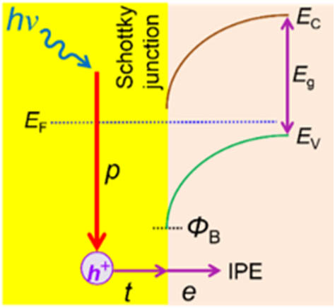
    Fig. 1. Energy band diagram of a metal contact to a p-type semiconductor and the three steps of the internal photoemission process: p, photoexcitation; t, transport; e, emission. EC and EV are the conduction and valence band edges, respectively, EF is the Fermi level, and ΦB is the Schottky barrier height.
    Schematic of an Au/p-Si optical antenna Schottky contact diode for sub-bandgap detection. The materials used are Au for the antennas, p-Si for the epitaxial layer, p+-Si for the substrate, and Au/Ti for the probing structure (pad and arm). The device is illuminated from the top with p-polarized IR light aligned along monopole lengths. A good design with a length of 125 nm, width of 44 nm, and thickness of 20 nm produces a resonant wavelength at λ=1534 nm, as identified from the computed absorptance response in the inset.
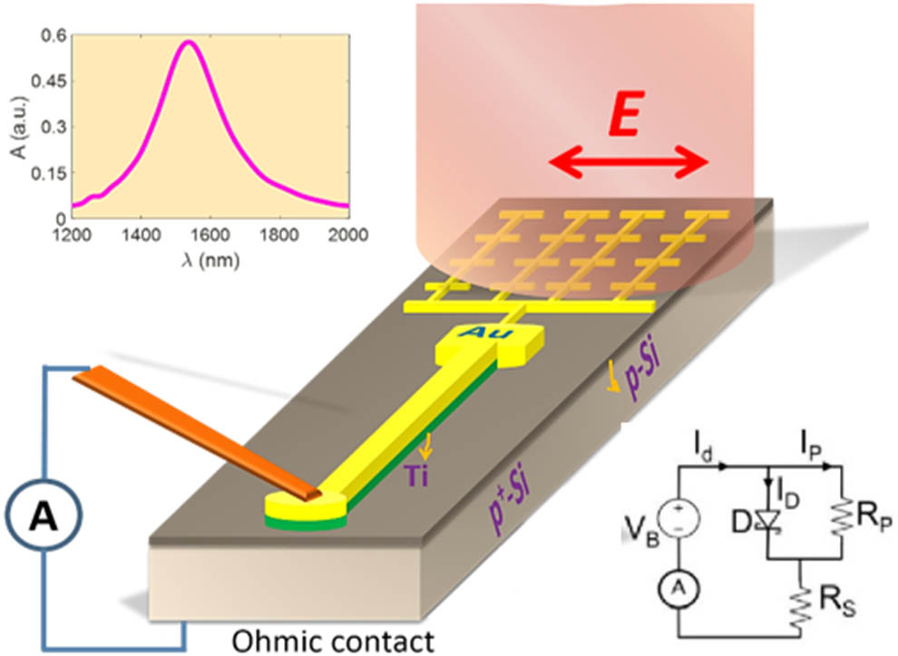
    Fig. 2. Schematic of an Au/p-Si optical antenna Schottky contact diode for sub-bandgap detection. The materials used are Au for the antennas, p-Si for the epitaxial layer, p+-Si for the substrate, and Au/Ti for the probing structure (pad and arm). The device is illuminated from the top with p-polarized IR light aligned along monopole lengths. A good design with a length of 125 nm, width of 44 nm, and thickness of 20 nm produces a resonant wavelength at λ=1534nm, as identified from the computed absorptance response in the inset.
    Sketch of the main steps developed and applied to fabricate electrically contacted antenna arrays.
    Fig. 3. Sketch of the main steps developed and applied to fabricate electrically contacted antenna arrays.
    (a) SEM image of a photoresist (S1805) lift-off resist (LOR-1A) stack after developing, showing a clean re-entrant profile. (b) E-beam layout of an antenna with its electrical interconnection line using structure redefinition to compensate for proximity effects. (c) Optical microscope image after e-beam writing and developing, showing an antenna array aligned with its electrical probing structure.
    Fig. 4. (a) SEM image of a photoresist (S1805) lift-off resist (LOR-1A) stack after developing, showing a clean re-entrant profile. (b) E-beam layout of an antenna with its electrical interconnection line using structure redefinition to compensate for proximity effects. (c) Optical microscope image after e-beam writing and developing, showing an antenna array aligned with its electrical probing structure.
    (a)–(d) SEM images of fabricated structures. (a) View of a full structure comprising a bilayer of Au/Ti probing structure and an array of Au electrically contacted monopole antennas. (b), (c) Higher-magnification images of arrays. (d) Higher-magnification image of electrically contacted monopole antennas. (e) Atomic force microscope image of electrically contacted monopole antennas.
    Fig. 5. (a)–(d) SEM images of fabricated structures. (a) View of a full structure comprising a bilayer of Au/Ti probing structure and an array of Au electrically contacted monopole antennas. (b), (c) Higher-magnification images of arrays. (d) Higher-magnification image of electrically contacted monopole antennas. (e) Atomic force microscope image of electrically contacted monopole antennas.
    Black curve shows an average of five dark I–V characteristics for a complete device. The inset shows the dark I–V characteristics of the probing structure only.
    Fig. 6. Black curve shows an average of five dark I–V characteristics for a complete device. The inset shows the dark I–V characteristics of the probing structure only.
    Measured photocurrent response of two electrically contacted monopole array photodetectors (VB=−10 mV). The monopoles are 45 nm wide, 17 nm thick, and (a) 124 nm long or (b) 130 nm long. The rapid wavelength variations correspond to Fabry–Perot resonances.
    Fig. 7. Measured photocurrent response of two electrically contacted monopole array photodetectors (VB=10mV). The monopoles are 45 nm wide, 17 nm thick, and (a) 124 nm long or (b) 130 nm long. The rapid wavelength variations correspond to Fabry–Perot resonances.
    Mohammad Alavirad, Anthony Olivieri, Langis Roy, Pierre Berini. Fabrication of electrically contacted plasmonic Schottky nanoantennas on silicon[J]. Chinese Optics Letters, 2018, 16(5): 050007
    Download Citation