1Department of Electronics, Carleton University, 1125 Colonel By Drive, Ottawa, Ontario K1S 5B6, Canada
2Centre for Research in Photonics, University of Ottawa, 25 Templeton Street, Ottawa, Ontario K1N 6N5, Canada
3Department of Electrical, Computer and Software Engineering, University of Ontario Institute of Technology, 2000 Simcoe Street North Oshawa, Ontario L1H 7K4, Canada
4School of Electrical Engineering and Computer Science, University of Ottawa, 800 King Edward Avenue, Ottawa, Ontario K1N 6N5, Canada
5Department of Physics, University of Ottawa, 150 Louis Pasteur, Ottawa, Ontario K1N 6N5, Canada
Mohammad Alavirad, Anthony Olivieri, Langis Roy, Pierre Berini. Fabrication of electrically contacted plasmonic Schottky nanoantennas on silicon[J]. Chinese Optics Letters, 2018, 16(5): 050007
Copy Citation Text
We fabricate Schottky contact photodetectors based on electrically contacted Au nanoantennas on p-Si for the plasmonic detection of sub-bandgap photons in the optical communications wavelength range. Based on a physical model for the internal photoemission of hot carriers, photons coupled onto the Au nanoantennas excite resonant plasmons, which decay into energetic “hot” holes emitted over the Schottky barrier at the Au/p-Si interface, resulting in a photocurrent. In our device, the active Schottky area consists of Au/p-Si contact and is very small, whereas the probing pad for external electrical interconnection is larger but consists of Au/Ti/p-Si contact having a comparatively higher Schottky barrier, thus producing negligible photo and dark currents. We describe fabrication that involves an electron-beam lithography step overlaid with photolithography. This highly compact component is very promising for applications in high-density Si photonics.
Plasmonic nanoantennas have become important photonic components for several applications involving the conversion of light from free-space to small sub-wavelength volumes. The behavior of metals at optical frequencies is different from the microwave regime, and this creates differences between optical antennas and microwave antennas[1,2]. Well-designed metallic structures having small dimensions, narrow gaps, and sharp corners produce significant local optical field enhancement and, consequently, strong enhancement of light–matter interaction. Conversely, larger structures have better scattering-to-extinction cross-section ratios and better responses in the far-field. Optical nanoantenna designs must trade-off these properties[3]. Nanoscale monopoles, dipoles, and bowties are three of the most popular types of optical antennas. In most cases, Au and Ag are used as the metals for the antennas, typically on a glass, indium tin oxide (ITO), or Si substrate. The range of applications of these types of antennas is very broad: biosensing[4,5], photodetection[6], spectroscopy and imaging[7], and waveguiding[8] are some examples.
The electric near-fields produced by optical antennas can be of much greater intensity than the incident electric fields[9], so the photodetection volume can shrink, leading to faster devices with compelling signal-to-noise characteristics[10]. Mousavi et al. investigated a surface plasmon polariton (SPP) photodetector based on the enhancement of electric near-fields in low-defect, low-doped detection volumes located in the gaps of an array of metal dipole antennas[11]; significant enhancement in responsivity was attributed to the dipoles. The 3 dB electrical bandwidth of the device was estimated based on its resistor-capacitor (RC) rise time and the hole transit time through the detection volume for the cases of conventional and ballistic transport and was found to range from to 4 THz. Monopole arrays were also investigated for photodetection based on internal photoemission (IPE)[9]. The systems investigated consist of Au nanowires on Si covered by and a thin adlayer, representing a biochemical coating aiming towards biosensing applications. The resonance excited on such antennas by perpendicularly incident light polarized along their axis is dipolar and comprised of an SPP waveguide mode propagating along the length of the nanowires and reflecting from the ends to form standing waves along the antenna[12]. The waveguide mode excited on the nanowires is a mode of an asymmetric metal stripe[13].
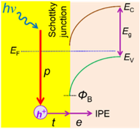
The IPE mechanism for holes is sketched in Fig. 1. IPE is a three-step process consisting of the photoexcitation of hot (energetic) carriers in the metal, transport with scattering of hot carriers towards the metal–Si interface, and the emission of hot carriers over the Schottky barrier into the semiconductor, where they are collected as the photocurrent. IPE requires that the energy of the incident photons ( is Planck’s constant and is the optical frequency) be greater than that of the Schottky barrier . This mechanism is useful for detection at energies below the semiconductor bandgap .
Sign up for Chinese Optics Letters TOC. Get the latest issue of Chinese Optics Letters delivered right to you!Sign up now
Figure 1.Energy band diagram of a metal contact to a p-type semiconductor and the three steps of the internal photoemission process: , photoexcitation; , transport; , emission. and are the conduction and valence band edges, respectively, is the Fermi level, and is the Schottky barrier height.
In this Letter, we present the fabrication of IPE-based Schottky detectors, where the contact electrode is formed as electrically contacted metal monopoles. The device uses hot holes arising from plasmon decay to generate the photocurrent, resulting in the detection of sub-bandgap infrared (IR) light. To reduce the dark current, we fabricated the probing structure as a metal bilayer Au/Ti of a higher Schottky barrier than the Au antenna array.
Design. Fig. 2 shows a schematic of the structure of interest. It consists of an array of monopoles (thickness ) for guiding SPPs on a lightly doped p-Si epitaxial layer on a heavily doped substrate. The Au monopoles are interconnected via Au lines running perpendicular to their axes through the middle of each to a common circular contact pad used to collect the photocurrent. The monopoles are designed to couple normally incident -polarized IR (, sub-bandgap) light to SPPs propagating along their bottom surface, such that the SPP fields are coincident with the Schottky contact. As SPPs propagate, they are absorbed in the metal, generating hot carriers therein, primarily along the Schottky contact. Detection then occurs through the collection of hot holes in p-Si via IPE. The substrate is placed on a backside Al ohmic ground contact.
Figure 2.Schematic of an Au/p-Si optical antenna Schottky contact diode for sub-bandgap detection. The materials used are Au for the antennas, p-Si for the epitaxial layer, for the substrate, and Au/Ti for the probing structure (pad and arm). The device is illuminated from the top with -polarized IR light aligned along monopole lengths. A good design with a length of 125 nm, width of 44 nm, and thickness of 20 nm produces a resonant wavelength at , as identified from the computed absorptance response in the inset.
The proposed photodetector was analyzed by investigating its electromagnetic performance over a range of wavelengths. The inset to Fig. 2 shows the computed absorptance response for a good design with a length of 125 nm, width 44 nm, and thickness 20 nm. The array consisted of 1600 monopoles arranged in a matrix with a 300 nm inter-antenna spacing in both the longitudinal and transverse directions, sufficient to ensure that near-field inter-antenna coupling is absent, as verified via electromagnetic modelling. The computations were carried out using commercial software implementing the finite-difference time-domain (FDTD) method.
The dark current of a Schottky diode is given by where is Boltzmann’s constant, is the ideality factor, is the absolute temperature, is the effective Richardson constant ( for holes[14]), and is the Schottky contact area. The probing structure (pad and arm) is made of Au/Ti in order to reduce its dark current (Ti produces a significantly higher Schottky barrier on p-Si than Au). The dark current is then determined by the sum of two terms: one due to the Au/Ti probing structure and the other by the Au monopole array. The contact areas are for the Au/Ti/p-Si structure and for the Au/p-Si electrically contacted monopole array. Dark currents of and 3.8 μA are expected, respectively, at 300 K. The low barrier height of the monopole array should permit a detection window covering the entire shortwave IR spectral range ( to 2.5 mm).
Fabrication. Figure 3 describes the main steps developed and applied to fabricate the devices. The devices were fabricated on a double-side polished wafer, consisting of a substrate thick, of acceptor density to , bearing a p-Si epitaxial layer thick, of acceptor density to .
Figure 3.Sketch of the main steps developed and applied to fabricate electrically contacted antenna arrays.
Sintered Al was used for the ohmic contact on the backside. A 2 in. (1 in. = 2.54 cm) wafer was dipped in buffered oxide etch [BOE, ammonium fluoride–hydrofluoric (HF) acid mixture, Aldrich, AF 875-125] for 30 s to remove any native oxide growth and then placed in an evaporator to deposit 1 μm of Al on the backside. The wafer was then sintered at 700°C, forming an ohmic contact. The wafer was again dipped in BOE for 30 s to remove any oxide growth; then 100 nm of Au was sputtered (Quorum 150 R) on the Al ohmic contact to protect it from oxidizing and from subsequent exposure to Microposit, MF-321 developer (Microchem).
The Au/Ti probing structures were fabricated on the p-Si epitaxial surface using a bilayer lift-off photolithography technique. A lift-off resist (LOR)-1A (Microchem) layer was spun at 3000 r/min (WS-650-23NPP, Laurell) and then baked at 180°C for 5 min. The LOR-1A thickness measured with a profilometer (DektakXT, Bruker) was 175 nm. S1805 photoresist (Microchem) was then spun at 6000 r/min and baked at 120°C for 5 min. The S1805 thickness was measured to be 550 nm. The LOR-1A/S1805 photoresist stack was exposed with a UV mask aligner (Hybralign Series 200IR, OAI) for 5.0 s at a lamp intensity of [Fig. 3(a)]. The exposed photoresist stack was then developed at room temperature suspended upside down in MF-321 for 2 min with ultrasonic agitation (80 kHz) (FB11201, Fisherbrand), rinsed with distilled (DI) , and dried with . A scanning electron microscope (SEM, GeminiSEM 500, Ziess) cross-section of a developed feature in the stack can be seen in Fig. 4(a), showing a clean re-entrant profile. The wafer was immediately placed into an evaporator (NexDep, Angstrom). Under a chamber vacuum of , 5 nm of Ti was evaporated via an electron-beam (e-beam) at 2 Å/s (1 Å = 0.1 nm) [Fig. 3(b)]. Without breaking vacuum, 15 nm of Au was then thermally evaporated at 0.5 Å/s [Fig. 3(c)]. The Ti layer is intended to reduce the dark current, but also to make the devices more robust for electrical probing during testing. An Au/Ti stack was used to make the features readily observable under the SEM for the subsequent overlaid e-beam lithography step (Ti is hard to image under SEM). Lift-off was carried out in propylene glycol (PG) remover (G516604, Microchem) for 30 min, followed by rinses in acetone (270725, Sigma-Aldrich), isopropyl alcohol (IPA, Isopropanl-2, 733458, Sigma-Aldrich), and DI , and dried with [Fig. 3(d)]. The wafer was then baked on a hotplate at 200°C for 1 h.
Figure 4.(a) SEM image of a photoresist (S1805) lift-off resist (LOR-1A) stack after developing, showing a clean re-entrant profile. (b) E-beam layout of an antenna with its electrical interconnection line using structure redefinition to compensate for proximity effects. (c) Optical microscope image after e-beam writing and developing, showing an antenna array aligned with its electrical probing structure.
The layout of the electrically contacted Au monopole arrays was prepared using e-LiNE software[15], and e-beam lithography was used to define them in a bilayer polymethyl methacrylate (PMMA) lift-off process. The layout of the arrays overlapped with the probing structures to ensure electrical continuity. Proximity effect correction was done via structural redefinition. Figure 4(b) shows a 120 nm long, 25 nm wide single antenna with a 30 nm wide electrical interconnection line. Extra squares in the corners of the antennas compensate for the proximity effect, as corners will receive less of a dose, so they typically end up with large radii of curvature. The converse is also true, as junctions or inside corners will receive a higher dose, so areas are subtracted from intersections with the interconnection lines.
A PMMA (Microchem) bilayer was deposited on the wafer. The first layer was 495K PMMA 2% solid content, spun at 6000 r/min, and then cured at 200°C for 1 h. The measured thickness of the first layer is 40–50 nm. A second layer of 950K PMMA 2% solid content was then spun at 6000 r/min and cured at 200°C for 1 h.
The e-beam lithography was done with a Raith Pioneer system at an acceleration voltage of 30 kV with a 10 μm aperture, resulting in a beam current of 30 pA. A single dosage of was used to define all structures. The exposure time per antenna array was 1 to 2 min [Fig. 3(e)]. The sample was then developed in methyl isobutyl ketone (MIBK):IPA (1:3, Microchem) at 20°C for 2 min, rinsed in IPA, and then dried with [Fig. 3(f)].
The sample was inspected with an optical microscope (Axio Imager, Zeiss), as shown in Fig. 4(c). Although individual antennas are not resolvable with such a microscope, the larger features and the array alignments are, so they can be verified before Au deposition. The sample was then dipped in BOE for 30 s to remove any native , rinsed in DI , dried with , and immediately placed into the evaporator under vacuum. 20 nm of Au was thermally deposited at a rate of 0.5 Å/s in a chamber vacuum of [Fig. 3(g)]. Lift-off was then performed in acetone for and then under 80 kHz ultrasonic agitation for 30 s [Fig. 3(h)]. The sample was then rinsed with IPA and dried. No cover layer was used to allow for direct electrical probing and photocurrent measurements.
Figures 5(a)–5(d) show SEM images of fabricated structures. The metal thickness and roughness were deduced from atomic force microscope (AFM) scans of the antenna array, as shown in Fig. 5(e), revealing a thickness of with a root mean square (RMS) roughness of 1 nm for each monopole (design target of ). All other dimensions are well in keeping with the target ones.
Figure 5.(a)–(d) SEM images of fabricated structures. (a) View of a full structure comprising a bilayer of Au/Ti probing structure and an array of Au electrically contacted monopole antennas. (b), (c) Higher-magnification images of arrays. (d) Higher-magnification image of electrically contacted monopole antennas. (e) Atomic force microscope image of electrically contacted monopole antennas.
Measurements. A photodetector under test is biased by probing its probe pad and grounding its Al contact using a source meter (Fig. 2). A cleaved polarization-maintaining single-mode fiber (PM-SMF) is used to excite the photodetector under test from the top. A tunable external cavity laser is used to generate the incident light at . Instrument control and data acquisition are performed via computer using LabVIEW (SP1 2013)[16]. The optical power incident on a photodetector is determined by removing the losses of all the elements in the input path of the setup.
The experiments were conducted by placing a die under test under microscope and using tipless AFM cantilever probes attached to a micro-positioner to make electrical contact to a device on its probe pad. Another micro-positioner is then used to align the PM-SMF (-polarization aligned) to the photodetector. When the fiber is rotated to produce -polarized incidence, almost no photocurrent is generated. All measurements were obtained at room temperature.
The black curve in Fig. 6 shows an average of five measured I–V curves for a Schottky photodetector without illumination. It shows the rectifying property of the Schottky structure. The reverse bias characteristics are soft for all tested antenna devices due to the low Schottky barrier and possibly to deep traps formed by the diffusion of Au into p-Si during fabrication[17]. The total contact area of our test device is . To obtain a lower dark current, we designed and fabricated the probing structure as a bilayer of Au/Ti, which forms a higher Schottky barrier on p-Si than Au. The area of the probing structure is , which corresponds to more than 90% of the entire device area. Taking for Ti/p-Si, and for Au/p-Si[14] produces for the Ti/p-Si probing structure, and for the Au/p-Si electrically contacted antenna array. The dark current in this structure is five times lower than for the corresponding Au-only design, resulting in an improved signal-to-noise ratio (SNR) for the photodetector.
Figure 6.Black curve shows an average of five dark I–V characteristics for a complete device. The inset shows the dark I–V characteristics of the probing structure only.
Solving Eq. (1) to obtain from the measurements is not very accurate because the experimental setup and the photodetectors have a high resistance. The reverse bias and small forward bias regimes are affected by the shunt current and the shunt and series resistances and of the equivalent circuit of a non-ideal diode[17], as sketched in the bottom left inset of Fig. 2. Several methods can be applied to extract the barrier height of high-resistance Schottky diodes. The method proposed by Werner[18] has been shown to yield accurate results. Following this method yields , , and , . The ideality factor was found to be 3.18 and 0.91 for Au/p-Si and Ti/p-Si, respectively. Given that must be satisfied in order for the SPPs to be detected, the long-wavelength cut-off of the photodetectors is , implying a broad range of operating wavelengths limited only by the antenna design.
Figure 7 plots the -polarized photocurrent response measured at normal incidence with , and for two detectors having arrays of monopoles of different dimensions. Two wavelength dependencies are observed on each response. The rapidly varying dependencies come from Fabry–Perot resonances.
Figure 7.Measured photocurrent response of two electrically contacted monopole array photodetectors (). The monopoles are 45 nm wide, 17 nm thick, and (a) 124 nm long or (b) 130 nm long. The rapid wavelength variations correspond to Fabry–Perot resonances.
In summary, we have presented a broadband Si plasmonic Schottky photodetector operating in the sub-bandgap regime and exploiting IPE. A monopole antenna array is used to couple perpendicularly incident light to SPPs propagating along an array of Au monopoles forming a Schottky contact to p-Si. The response is enhanced by the absorption of SPPs directly along the Schottky contact, leading to the creation of hot holes near the contact. These holes cross over the Schottky barrier () and are collected as a photocurrent.
Mohammad Alavirad, Anthony Olivieri, Langis Roy, Pierre Berini. Fabrication of electrically contacted plasmonic Schottky nanoantennas on silicon[J]. Chinese Optics Letters, 2018, 16(5): 050007