Bing Liu, Xuping Wang, Yuguo Yang, Yanyan Hu, Huajian Yu, Fengnian Wu. Principles, Devices, and Applications of Beam Deflection Based on Quadratic Electro-Optic Effect of Potassium Tantalate Niobate[J]. Laser & Optoelectronics Progress, 2020, 57(7): 071609
Search by keywords or author
- Laser & Optoelectronics Progress
- Vol. 57, Issue 7, 071609 (2020)
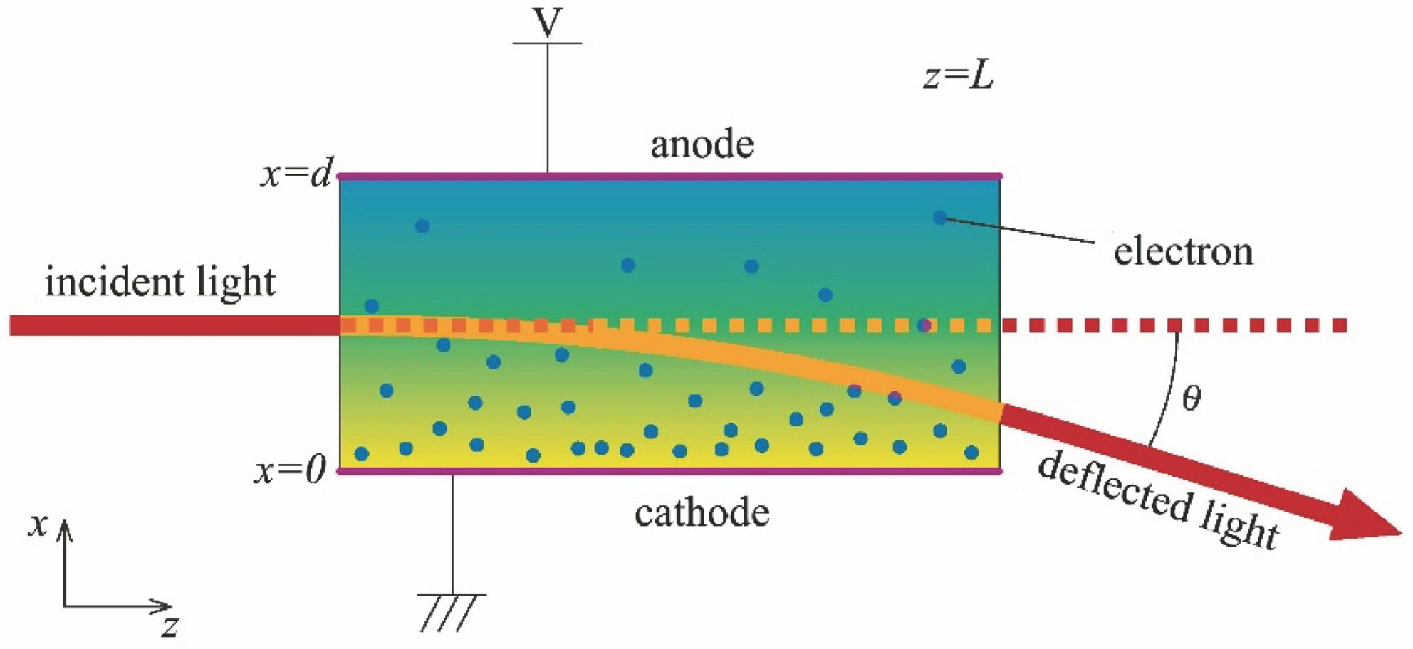
![Space-charge-controlled electro-optic deflection[52]](/richHtml/lop/2020/57/7/071609/img_1.jpg)
Fig. 1. Space-charge-controlled electro-optic deflection[52]
![Voltage profile of new electro-optic deflection model[30]](/richHtml/lop/2020/57/7/071609/img_2.jpg)
Fig. 2. Voltage profile of new electro-optic deflection model[30]
Fig. 3. Deflection angle as a function of applied voltage at 100 kHz[30]
Fig. 4. Schematic of electro-optic deflection based on KTN composition gradient[45]
Fig. 5. Variation in electro-optic deflection angle with applied voltage based on KTN composition gradient[45]
Fig. 6. Diagram of temperature gradient of KTN[37]
Fig. 7. Temperature gradient induced electro-optic deflection angle varies with applied voltage[63]
Fig. 8. KTN electro-optic deflector with multiple reflection structure. (a) Reflection for twice[65] (b) reflection for six times[66]
Fig. 9. Quadratic electro-optic coefficient as a function of temperature at different cooling rates[34]
Fig. 10. Response time of electro-optic rotation of KTN crystal at different temperature[38]
Fig. 11. Number of resolvable points for electro-optic deflector[65]
Fig. 12. Tracing result of deflected beam of KTN[73]. (a) Beam distortion; (b) beam shaping
Fig. 13. Power consumption versus frequency[77]
Fig. 14. Schematic diagram of KTN deflector[66]
Fig. 15. Space charge density distributions in KTN with applied voltage[79]. (a) With different voltages; (b) with different permittivities
Fig. 16. Electron penetration depth as a function of time[82]
Fig. 17. Size of PNRs versus temperature[69]
Fig. 18. D-E curves of KTN crystal with platinum electrode[88]
Fig. 19. Deflection angle caused by field-induced phase transition varies with applied voltage[90]
Fig. 20. Deflection angle at different positions in x direction with 2000 V applied voltage[39]
Fig. 21. Illustration of KTN varifocal lens[95].(a)Apparatus; (b)optical path length at different positions in x direction
Fig. 22. Schematic of experimental setup for 1×5 optical switch[104]
Fig. 23. Electric-field-induced superlattice optical switching effect in Cu-doped KTN crystals[106]. (a) Diffraction spot induced by spontaneously formed superlattices; (b)(c) optical switching states of diffraction spot with 1 Hz square-wave voltage
Fig. 24. Setup of swept light source with KTN electro-optic deflector[33]
Fig. 25. 3D OCT image of strawberry surface[109]
Fig. 26. Schematic of spectrometer using KTN optical beam deflector[110]
Fig. 27. Spatial overlap modulation nonlinear optical microscopy[112]
Fig. 28. Illustration of time division multiplexed beam combining technique[113]
|
Table 1. Damage thresholds of several optical crystals

Set citation alerts for the article
Please enter your email address


