Alessandro Tuniz, Markus A. Schmidt, Boris T. Kuhlmey, "Influence of non-Hermitian mode topology on refractive index sensing with plasmonic waveguides," Photonics Res. 10, 719 (2022)

Search by keywords or author
- Photonics Research
- Vol. 10, Issue 3, 719 (2022)
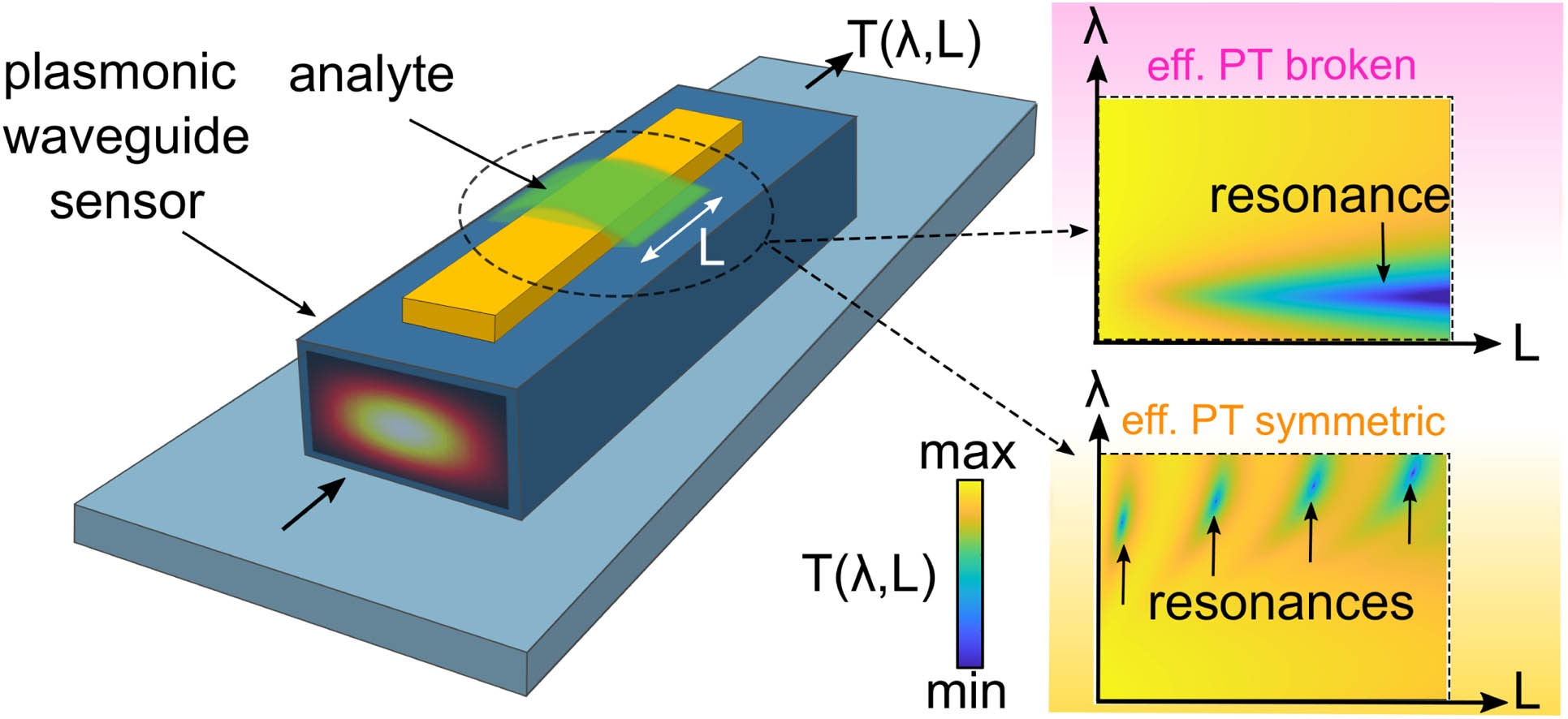
![Concept schematic overview of the present study. A plasmonic waveguide sensor can be used to identify change in the refractive index of an analyte (blue: dielectric; yellow: metal; green: analyte; interaction length: L) by coupling to a mode at the input and measuring the transmission spectrum T at the output. Note that the resonant transmission is a function of both wavelength λ and length L and can present remarkably different characteristics depending on whether the system is in the EPTS or EPTB regime [18], each unlocked by changing the refractive index of the analyte.](/richHtml/prj/2022/10/3/03000719/img_001.jpg)
Fig. 1. Concept schematic overview of the present study. A plasmonic waveguide sensor can be used to identify change in the refractive index of an analyte (blue: dielectric; yellow: metal; green: analyte; interaction length: L ) by coupling to a mode at the input and measuring the transmission spectrum T at the output. Note that the resonant transmission is a function of both wavelength λ and length L and can present remarkably different characteristics depending on whether the system is in the EPTS or EPTB regime [18], each unlocked by changing the refractive index of the analyte.
![Concept schematic of the plasmonic waveguide sensor considered. The fundamental mode input of a dielectric silica waveguide (width: d; field: ψin=ψ1d) couples to the hybrid EMs (ψ1,2, indicated by blue and red curves) of a gold-coated region (thickness: t), surrounded by a liquid of refractive index na. The EM excitation and interference over a length L result in a wavelength-dependent transmitted power T, which can contain information on changes in na. The output field is a superposition of the dielectric waveguide EMs, ψout=t1ψ1d+t2ψ2d+…. The sensing region is lossy and thus non-Hermitian. (b) Example T(λ) spectra for increasing na. The shift in resonant wavelength λR determines the sensitivity S=dλR/dna. Each resonance possesses a characteristic 3 dB-width δλ, which depends on EM excitation and interference upon propagation. Small changes in na can be resolved for small δλ and large S, i.e., the DL is δn∝δλ/S [31].](/richHtml/prj/2022/10/3/03000719/img_002.jpg)
Fig. 2. Concept schematic of the plasmonic waveguide sensor considered. The fundamental mode input of a dielectric silica waveguide (width: d ; field: ψ in = ψ 1 d ) couples to the hybrid EMs (ψ 1,2 , indicated by blue and red curves) of a gold-coated region (thickness: t ), surrounded by a liquid of refractive index n a . The EM excitation and interference over a length L result in a wavelength-dependent transmitted power T , which can contain information on changes in n a . The output field is a superposition of the dielectric waveguide EMs, ψ out = t 1 ψ 1 d + t 2 ψ 2 d + … . The sensing region is lossy and thus non-Hermitian. (b) Example T ( λ ) spectra for increasing n a . The shift in resonant wavelength λ R determines the sensitivity S = d λ R / d n a . Each resonance possesses a characteristic 3 dB-width δ λ , which depends on EM excitation and interference upon propagation. Small changes in n a can be resolved for small δ λ and large S , i.e., the DL is δ n ∝ δ λ / S [31].
![(a) Summary schematic of relevant modes. Solid blue/orange curves: hybrid modes of a silica waveguide of finite width in contact with a thin gold film. The blue dashed curve corresponds to an equivalent system without gold film (dielectric mode), and orange dashed curve corresponds to an equivalent system with infinite silica width (plasmonic mode). The associated ℜe(neff) (top row) and loss (in dB/μm, bottom row), as a function of wavelength, are shown for (b) na=1.32, (c) na=1.33, and (d) na=1.36. Note the transition from the crossing to anticrossing of ℜe(neff) [and vice versa for the loss via ℑm(neff)] via the EP. Also shown are different criteria used in the literature for inferring where plasmonic resonances occur: phase matching (where the real parts of the dielectric and plasmonic EMs cross [29]), maximum loss (where the loss of the dielectric-like hybrid mode is maximum [20]), and loss-matching [49] (where the imaginary parts of the hybrid EMs cross). The wavelength λΔneffmin of minimum effective index difference is also indicative of strong coupling [50]. In the present configuration and near resonance, eigenvalues coalesce at the EP when na=1.33, na<1.33 supports EPTB modes, and na>1.33 supports EPTS modes. (e) Detailed 3D plot of ℜe(neff) (top) and loss (bottom), as a function of wavelength and na.](/Images/icon/loading.gif)
Fig. 3. (a) Summary schematic of relevant modes. Solid blue/orange curves: hybrid modes of a silica waveguide of finite width in contact with a thin gold film. The blue dashed curve corresponds to an equivalent system without gold film (dielectric mode), and orange dashed curve corresponds to an equivalent system with infinite silica width (plasmonic mode). The associated ℜ e ( n eff ) (top row) and loss (in dB / μm , bottom row), as a function of wavelength, are shown for (b) n a = 1.32 , (c) n a = 1.33 , and (d) n a = 1.36 . Note the transition from the crossing to anticrossing of ℜ e ( n eff ) [and vice versa for the loss via ℑ m ( n eff ) ] via the EP. Also shown are different criteria used in the literature for inferring where plasmonic resonances occur: phase matching (where the real parts of the dielectric and plasmonic EMs cross [29]), maximum loss (where the loss of the dielectric-like hybrid mode is maximum [20]), and loss-matching [49] (where the imaginary parts of the hybrid EMs cross). The wavelength λ Δ n eff min of minimum effective index difference is also indicative of strong coupling [50]. In the present configuration and near resonance, eigenvalues coalesce at the EP when n a = 1.33 , n a < 1.33 supports EPTB modes, and n a > 1.33 supports EPTS modes. (e) Detailed 3D plot of ℜ e ( n eff ) (top) and loss (bottom), as a function of wavelength and n a .

Fig. 4. (a) Spectral distribution of power in the fundamental dielectric waveguide mode at output as a function of wavelength T ( λ ) = | t 1 ( λ ) | 2 , for the four analyte indices of Fig. 3 as labeled, for L = 25 μm , L = 37.5 μm , and L = 50 μm (blue, orange, and yellow, respectively). Dashed-dotted lines compute Eq. (4 ) for one example length (L = 37.5 μm ). (b) Total power in the waveguide at output as a function of wavelength, i.e., T ( λ ) = Σ i | t i ( λ ) | 2 . Solid lines correspond to calculations performed via the EM method (EMM), including mode excitation and propagation, and dashed lines correspond to full vector FEM calculations (COMSOL). Axial component of the normalized Poynting vector in the sensor region at resonance (c) in the EPTB regime (n a = 1.32 , λ R = 560 nm ) and (d) in the EPTS regime (n a = 1.36 , λ R = 610 nm ), calculated using FEM. Note that the color scale is linear.

Fig. 5. Calculated transmission spectra (single-mode output) as a function of n a and λ for different values of L . (a) L = 25 μm (blue); (b) L = 37.5 μm (orange); and (c) L = 50 μm (yellow); (d) associated λ R ; (e) δ λ ; and (f) T min . Line colors in (d)–(f) correspond to that of the L values labeled in (a)–(c). All plots are in the EPTS regime, where the smallest δ λ is achievable due to directional coupling.

Fig. 6. (a) Resonant wavelength λ R as a function of analyte index n a , obtained from full transmission calculations, for L = 25 μm (dark blue) and L = 37 μm (orange), corresponding to Fig. 5 (d). The gray shaded region shows the entire range of possible λ R for L = 10 – 200 μm . Cutoff wavelength (black), PM wavelength (light blue), loss-matching wavelength (purple), and wavelength for minimum effective index (green), as a function of analyte index, obtained from mode calculations, and as defined in Fig. 3 (b). Corresponding sensitivity S = d λ R / d n a for each curve in (a) log scale. The gray shaded region shows the entire range of possible S using λ R for L = 10 – 2000 μm .
![(a) Calculated transmission spectra (single-mode output) as a function of L and λ for different values of na as labeled, and (b) associated λR, (c) δλ, (d) Tmin. In (b)–(d), each curve’s color refers to the na labels in (a). For each na, we identify the first resonance dip at LR [dashed line in (d)], corresponding to half a beat length [28].](/Images/icon/loading.gif)
Fig. 7. (a) Calculated transmission spectra (single-mode output) as a function of L and λ for different values of n a as labeled, and (b) associated λ R , (c) δ λ , (d) T min . In (b)–(d), each curve’s color refers to the n a labels in (a). For each n a , we identify the first resonance dip at L R [dashed line in (d)], corresponding to half a beat length [28].

Fig. 8. (a) First resonance dip L R obtained from Fig. 7 (d). The wavelength λ R at which it occurs is shown in the inset. Note the rapid increase in L R close n a = 1.33 , corresponding to the EP. (b) EM splitting as a function of analyte permittivity perturbation Δ ε with respect to the EP at n a = 1.33 , obtained from the dispersion of Fig. 3 , and showing a characteristic square root dependence; inset, wavelength dependence of the EM splitting; (c) EM splitting estimated from the calculated transmission spectra of Fig. 7 . The ratio 1 2 λ R / L R follows a square root dependence on Δ ε for small perturbations.

Set citation alerts for the article
Please enter your email address