
Quanrun Chen, Tao Zhang. Light Source Layout Optimization and Performance Analysis of Indoor Visible Light Communication System[J]. Acta Optica Sinica, 2019, 39(4): 0406003
- Acta Optica Sinica
- Vol. 39, Issue 4, 0406003 (2019)
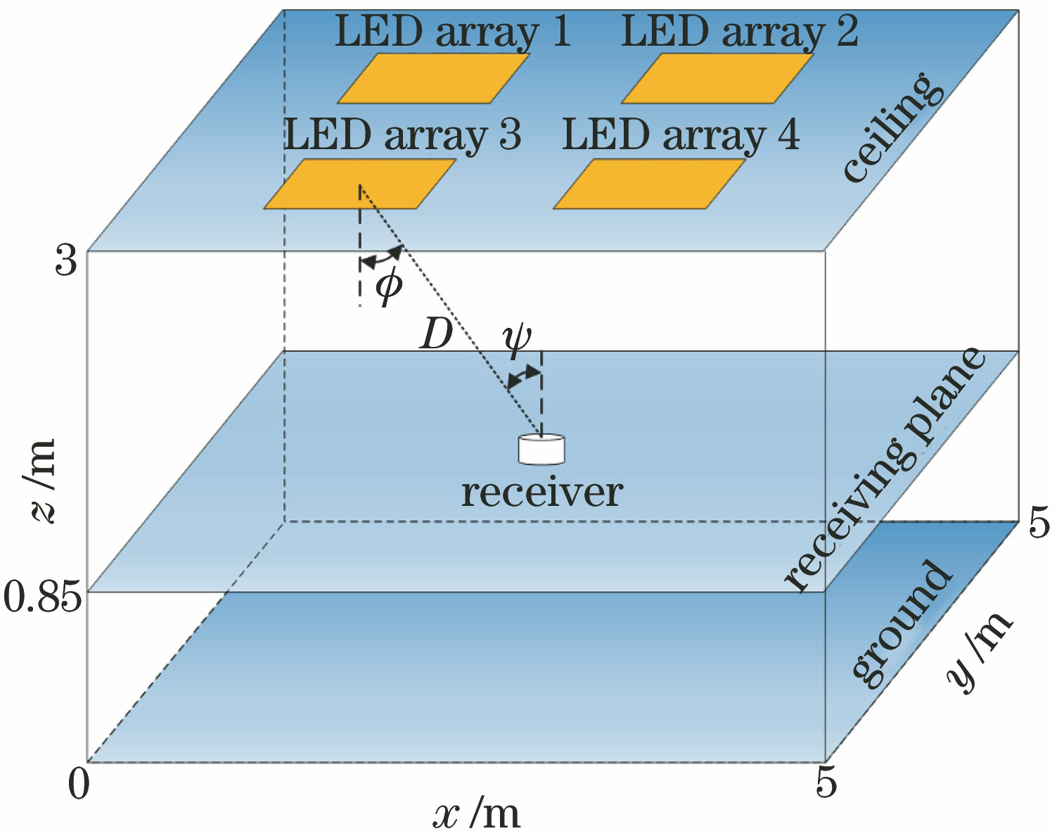
Fig. 1. Indoor VLC system model
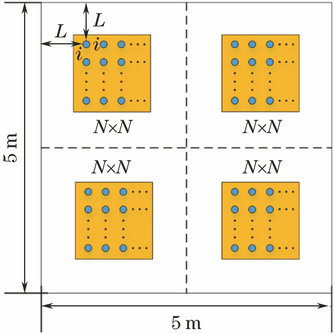
Fig. 2. Diagram of LED distribution in traditional square array layout
Fig. 3. Indoor impulse response distribution
Fig. 4. Diagram of LOS link and NLOS link
Fig. 5. Illuminance indices in traditional square array layout when N=8 and i=0.01 m. (a) Mean square deviation of illuminance at different L values; (b) distribution of illuminance on receiving surface when mean square deviation is minimum
Fig. 6. Illuminance indices in traditional square array layout under different (L, i) values when N=8. (a) Minimum illuminance distribution on receiving plane; (b) distribution of mean square deviation of illuminance on receiving plane
Fig. 7. Distribution of illuminance on receiving plane when L=1 m and i=0.04 m
Fig. 8. Light source layout model proposed by our team
Fig. 9. Illuminance indices in square array combined with circular ring layout under different (L, r) values when N1=7 and m1=12. (a) Distribution of minimum illuminance on receiving plane; (b) distribution of mean square deviation of illuminance on receiving plane
Fig. 10. Distribution of illuminance on receiving plane when L=1 m, r=0.1 m and i=0.03 m
Fig. 11. Illuminance indices on receiving plane obtained at the optimal (L, r) value and different LED intervals when N1=7 and m1=12. (a) Minimum illuminance; (b) maximum illuminance; (c) mean square error of illuminance; (d) uniformity of illuminance
Fig. 12. Illuminance indices on receiving plane obtained at optimal (L, r) value and different circular ring LED numbers when N1=7 and i=0.03 m. (a) Minimum illuminance value; (b) maximum illuminance value; (c) mean square error of illuminance; (d) uniformity of illuminance
Fig. 13. Illuminance distributions on receiving plane obtained at optimal (L, r) value in square array combined with circular ring layout. (a) N1=7, m1=8; (b) N1=7, m1=28
Fig. 14. Mean square deviation of illuminance on receiving plane obtained at different powers
Fig. 15. Power distributions on receiving plane obtained at optimal (L, r) value of square array combined with circular ring layout. (a) N1=7, m1=8; (b) N1=7, m1=12; (c) N1=7, m1=16; (d) N1=7, m1=20
Fig. 16. Received power distribution after power allocation at optimum (L, r) value when N1=7 and m1=12
Fig. 17. SNR and BER distributions on receiving plane obtained at the optimal (L, i) value in traditional square array layout when N=8. (a) SNR; (b) BER
Fig. 18. SNR and BER on receiving plane obtained after power allocation at the optimal (L, r) value when N1=7 and m1=12. (a) SNR; (b) BER
Fig. 19. Average BER versus height of receiving plane at different FOVs
Fig. 20. BER performance changes with system bandwidth and constellation maps. (a)Average BER versus modulation bandwidth at different modulation orders; (b) constellation map of 64QAM; (c) constellation map of 32QAM; (d) constellation map of 16QAM
|
Table 1. Simulation parameters

Set citation alerts for the article
Please enter your email address
© Copyright 2018-2021 | Chinese Laser Press. All Rights Reserved 沪ICP备15018463号-20