
Peihang Li, Peng Yu, Jiachen Sun, Zhimin Jing, Jiang Wu, Lucas V. Besteiro, Roberto Caputo, Arup Neogi, Hongxing Xu, Zhiming Wang, "Directional radiation enhancement of nanowire quantum dots based on line-array plasmonic antenna coupling," Photonics Res. 10, 2178 (2022)
- Photonics Research
- Vol. 10, Issue 9, 2178 (2022)
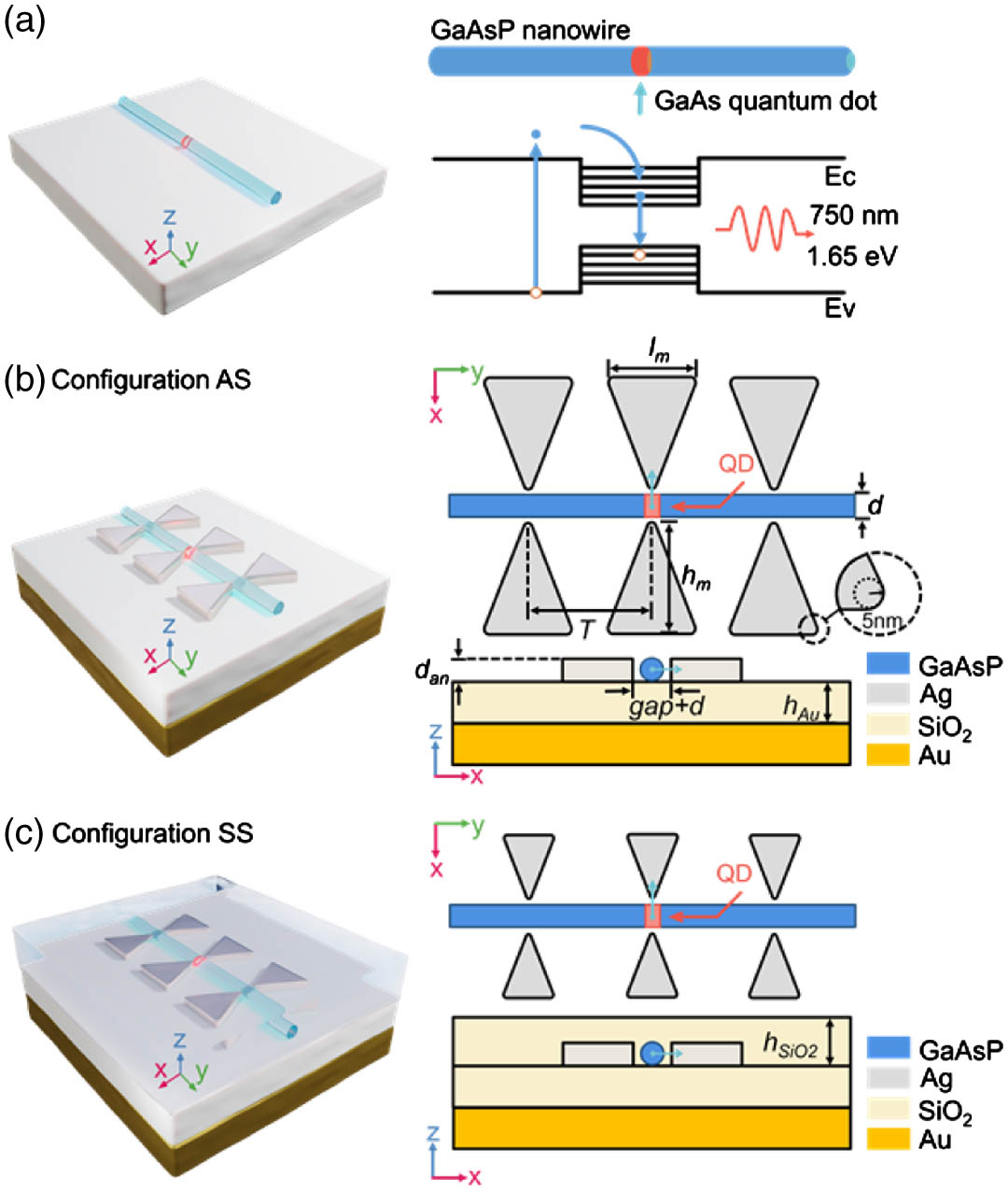
Fig. 1. (a) Schematic of the NWQD (left); schematic energy band diagram for the QD embedded in a nanowire (right). (b) Configuration AS, NWQD coupled to a line-array plasmonic bowtie nanoantenna in an air superstrate with a gold mirror. (c) Configuration SS, NWQD coupled to a line-array plasmonic bowtie nanoantenna in a SiO 2 d gap = 15 nm d an = 20 nm
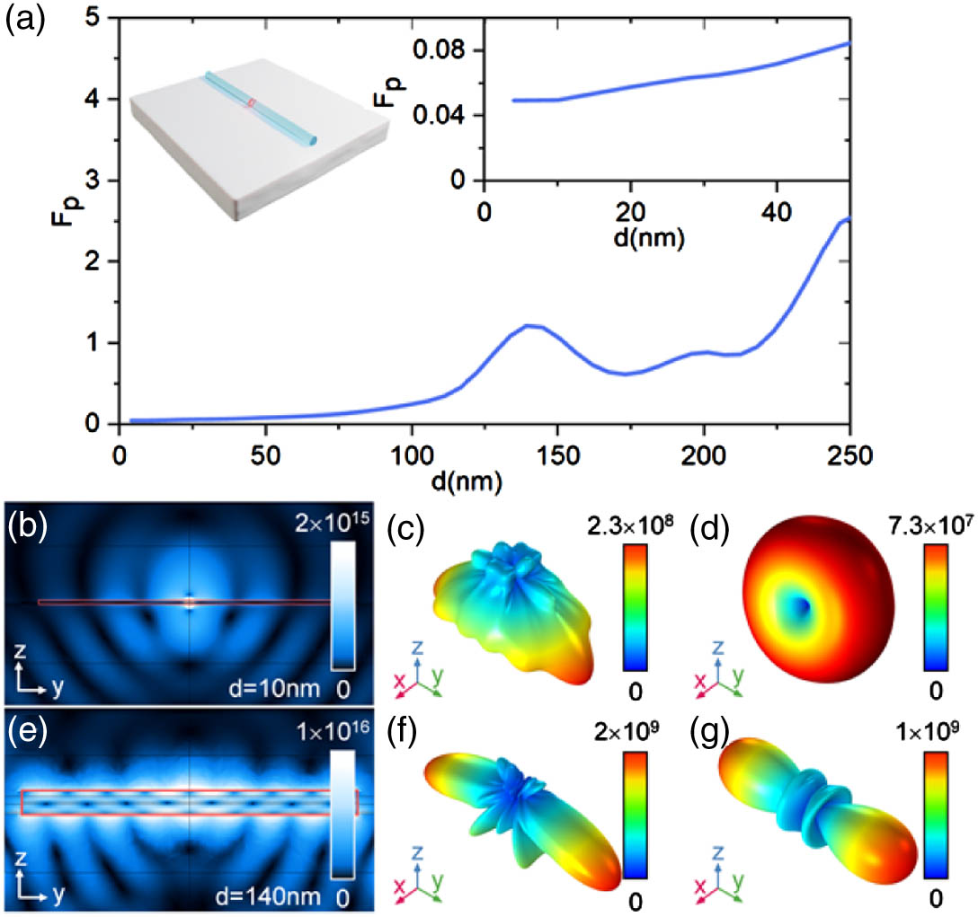
Fig. 2. (a) Trend of the variation of F p d d = 10 nm d = 10 nm d = 140 nm d = 140 nm
Fig. 3. (a) The NWQD coupled to a single plasmonic bowtie nanoantenna. (b) F p P L l m h m d = 10 nm d an = 20 nm
Fig. 4. (a) The NWQD coupled to a line-array plasmonic bowtie nanoantenna. (b) F p P L P L T T T = 420 nm
Fig. 5. (a) Electric field mode distributions of three pairs and a single plasmonic antenna under plane wave excitation. (b) Schematic diagram of single QD–line-array plasmonic antennas-coupled device. (c) Electric field mode distribution (V/m) and far-field radiation pattern (V/m) of single QD–line-array plasmonic antennas-coupled device, and the three red dots represent the tips of the three bowties.
Fig. 6. (a) Schematic diagram of a simplified mathematical model of the line-array antenna. (b) Main lobe directivity of the far-field radiation pattern of the simplified mathematical model of the line-array antenna. The inset is far-field patterns for different T
Fig. 7. (a) F p P L P L h Au h Au = 560 nm
Fig. 8. (a) F p P L P L h Au h Au = 560 nm
Fig. 9. Schematic diagram of the structure used in the physics simulation. Perfectly matched layers are placed outside the physical domain to simulate the propagation of electromagnetic waves in free space (absorbing electromagnetic waves to prevent reflected waves from affecting the structure itself).
Fig. 10. Influence of relative distance between the plasmonic antenna and the QD on enhancement effect.
Fig. 11. Distribution of electric field film (V/m) of five-pair plasmon antenna–NWQD coupling structure. Five-pair plasmon antenna–NWQD coupling structure electric field film distribution. The red outline is the NWQD, and the five red dots represent the tips of the three bowties.
Fig. 12. Effect of the relative errors of the NWQD and plasmonic antenna positions in the AS.
Fig. 13. Effect of the relative errors of the NWQD and plasmonic antenna positions in the SS.
Fig. 14. Collection efficiency of the SS with a different numerical aperture (NA).
Fig. 15. Collection efficiency of the AS with a different numerical aperture (NA).
Fig. 16. Performance effect of h SiO 2
Fig. 17. Far-field radiation pattern of the SS without gold mirrors with different h SiO 2 h SiO 2 = 40 nm h SiO 2 = 80 nm h SiO 2 = 160 nm h SiO 2 = 240 nm
|
Table 1. Comparison of SPE


Set citation alerts for the article
Please enter your email address

© Copyright 2018-2021 | Chinese Laser Press. All Rights Reserved 沪ICP备15018463号-20