• Photonics Research
  • Vol. 10, Issue 2, 594 (2022)
Haolin Li1、2、†, Xuanyu Zhang2、†, Haizhen Wang3, Jiahao Yu2, Kexue Li1, Zhipeng Wei1、4、*, Dehui Li3、5、*, and Rui Chen2、6、*
Author Affiliations
  • 1State Key Laboratory of High Power Semiconductor Laser, School of Science, Changchun University of Science and Technology, Changchun 130022, China
  • 2Department of Electrical and Electronic Engineering, Southern University of Science and Technology, Shenzhen 518055, China
  • 3School of Optical and Electronic Information and Wuhan National Laboratory for Optoelectronics, Huazhong University of Science and Technology, Wuhan 430074, China
  • 4e-mail: zpweicust@126.com
  • 5e-mail: dehuili@hust.edu.cn
  • 6e-mail: chenr@sustech.edu.cn
  • show less
    DOI: 10.1364/PRJ.444457 Cite this Article Set citation alerts
    Haolin Li, Xuanyu Zhang, Haizhen Wang, Jiahao Yu, Kexue Li, Zhipeng Wei, Dehui Li, Rui Chen. Optical characteristics of self-trapped excitons in 2D (iso-BA)2PbI4 perovskite crystals[J]. Photonics Research, 2022, 10(2): 594 Copy Citation Text show less
    (a) Schematic crystal structure of (iso−BA)2PbI4 crystals. (b) Photograph of as-synthesized (iso−BA)2PbI4 crystals. (c) Room-temperature absorption and PL spectra of (iso−BA)2PbI4 crystals. (d) PL spectra of (iso−BA)2PbI4 crystals under different excitation wavelengths.
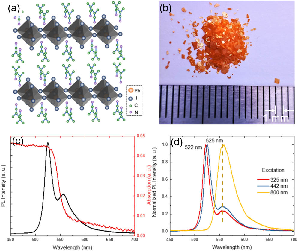
    Fig. 1. (a) Schematic crystal structure of (isoBA)2PbI4 crystals. (b) Photograph of as-synthesized (isoBA)2PbI4 crystals. (c) Room-temperature absorption and PL spectra of (isoBA)2PbI4 crystals. (d) PL spectra of (isoBA)2PbI4 crystals under different excitation wavelengths.
    (a) Low temperature PL emission of (iso−BA)2PbI4 crystals under different excitation intensities. The inset shows normalized spectra. (b) Integrated PL intensity of two emission peaks under different excitation powers. (c) Low temperature PL emission of (iso−BA)2PbI4 crystals under different excitation intensities. The inset shows normalized spectra. (d) Integrated PL intensity of two emission peaks under different excitation powers.
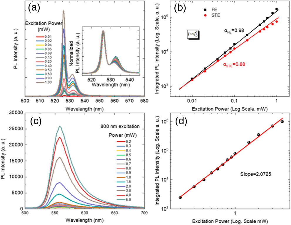
    Fig. 2. (a) Low temperature PL emission of (isoBA)2PbI4 crystals under different excitation intensities. The inset shows normalized spectra. (b) Integrated PL intensity of two emission peaks under different excitation powers. (c) Low temperature PL emission of (isoBA)2PbI4 crystals under different excitation intensities. The inset shows normalized spectra. (d) Integrated PL intensity of two emission peaks under different excitation powers.
    (a) Normalized temperature dependent PL spectra from 40 to 300 K. (b) Peak positions of FEs and STEs as a function of temperature. The solid lines are the fitting curves with Eq. (1) described in text. (c) FWHM of FEs and STEs as a function of temperature. The solid lines are the fitting curves with Eq. (2) described in text.
    Fig. 3. (a) Normalized temperature dependent PL spectra from 40 to 300 K. (b) Peak positions of FEs and STEs as a function of temperature. The solid lines are the fitting curves with Eq. (1) described in text. (c) FWHM of FEs and STEs as a function of temperature. The solid lines are the fitting curves with Eq. (2) described in text.
    (a) Integrated PL intensity (normalized) of samples at different temperatures. The solid lines are the fitting curves with Eq. (3). The inset shows the ratio of integrated PL intensity of two emissions (IEF/ISTE) at different temperatures. (b) Schematic energy level structure. GS, ground state; FE, free exciton state; FC, free carrier state; STE, self-trapped exciton state; Eg, band energy; Ef−s, trapping barrier energy; Es−f, detrapping barrier energy; Ed, lattice deformation energy.
    Fig. 4. (a) Integrated PL intensity (normalized) of samples at different temperatures. The solid lines are the fitting curves with Eq. (3). The inset shows the ratio of integrated PL intensity of two emissions (IEF/ISTE) at different temperatures. (b) Schematic energy level structure. GS, ground state; FE, free exciton state; FC, free carrier state; STE, self-trapped exciton state; Eg, band energy; Efs, trapping barrier energy; Esf, detrapping barrier energy; Ed, lattice deformation energy.
    (a) Microscope PL with different distances between objective lens and material surface. The inset shows PL photos of the sample in light and dark fields. (b) Schematic microscopy fluorescent system. (c) Optical photos of samples with different thicknesses; red arrow indicates the position of laser excitation. The thicknesses of samples 1–4 gradually increase. (d) PL spectra of samples with different sample thicknesses.
    Fig. 5. (a) Microscope PL with different distances between objective lens and material surface. The inset shows PL photos of the sample in light and dark fields. (b) Schematic microscopy fluorescent system. (c) Optical photos of samples with different thicknesses; red arrow indicates the position of laser excitation. The thicknesses of samples 1–4 gradually increase. (d) PL spectra of samples with different sample thicknesses.
    (a) Relative integrated intensity (IEF/ISTE) of two PL peaks at different positions of the same sample. The inset shows normalized spectra. (b) Excitation spot at different positions of the same sample.
    Fig. 6. (a) Relative integrated intensity (IEF/ISTE) of two PL peaks at different positions of the same sample. The inset shows normalized spectra. (b) Excitation spot at different positions of the same sample.
    Haolin Li, Xuanyu Zhang, Haizhen Wang, Jiahao Yu, Kexue Li, Zhipeng Wei, Dehui Li, Rui Chen. Optical characteristics of self-trapped excitons in 2D (iso-BA)2PbI4 perovskite crystals[J]. Photonics Research, 2022, 10(2): 594
    Download Citation