• Photonics Research
  • Vol. 10, Issue 2, 594 (2022)
Haolin Li1、2、†, Xuanyu Zhang2、†, Haizhen Wang3, Jiahao Yu2, Kexue Li1, Zhipeng Wei1、4、*, Dehui Li3、5、*, and Rui Chen2、6、*
Author Affiliations
  • 1State Key Laboratory of High Power Semiconductor Laser, School of Science, Changchun University of Science and Technology, Changchun 130022, China
  • 2Department of Electrical and Electronic Engineering, Southern University of Science and Technology, Shenzhen 518055, China
  • 3School of Optical and Electronic Information and Wuhan National Laboratory for Optoelectronics, Huazhong University of Science and Technology, Wuhan 430074, China
  • 4e-mail: zpweicust@126.com
  • 5e-mail: dehuili@hust.edu.cn
  • 6e-mail: chenr@sustech.edu.cn
  • show less
    DOI: 10.1364/PRJ.444457 Cite this Article Set citation alerts
    Haolin Li, Xuanyu Zhang, Haizhen Wang, Jiahao Yu, Kexue Li, Zhipeng Wei, Dehui Li, Rui Chen. Optical characteristics of self-trapped excitons in 2D (iso-BA)2PbI4 perovskite crystals[J]. Photonics Research, 2022, 10(2): 594 Copy Citation Text show less

    Abstract

    Organic–inorganic halide metal perovskites are an exciting class of two-dimensional (2D) materials that have sparked renewed interest for next-generation optoelectronics. In particular, the self-trapped excitons (STEs) in 2D perovskite with excellent optical properties suggest great potential in display and narrowband detection. A prerequisite of understanding STEs’ properties is correct identification of the underlying interaction that leads to STEs. Here, the optical properties of STEs in (iso-BA)2PbI4 are characterized through laser spectroscopy at various temperatures and excitation intensities. It is found that STEs are related to the octahedral distortion caused by strong electron–phonon interaction. Trapping and detrapping between STEs and free excitons (FEs) are clearly observed. With the increase in temperature, STEs and FEs will gain enough energy and migrate to each other. Moreover, by characterizing the thickness-dependent and two-photon excitation emission, it is confirmed that STEs exist inside the material because of their weak absorption. Our findings are of great significance for not only the fundamental understanding of STEs, but also the design and optimization of 2D-perovskite-based electronic and optoelectronic devices.

    1. INTRODUCTION

    Organic–inorganic halide metal perovskites have attracted tremendous interest due to their high power conversion efficiency and convenient synthesis. Although significant progresses have been achieved in perovskite-based optoelectronic devices, the stability issue of materials in ambient environment prevents their commercialization. In contrast, the emerging Ruddlesden–Popper two-dimensional (2D) perovskites have received increasing attention owing to their superior ambient stability and optoelectronic properties. In this structure, organic chains are inserted between inorganic octahedral sheets, so that the inorganic layers can prevent moisture in the air. Moreover, the unique architecture represents a natural quantum well structure due to the energy difference between organic and inorganic layers [14]. Due to the quantum confinement effect, the exciton binding energy of 2D perovskites can be as large as hundreds of meV [5]. The layered structure of the 2D perovskite provides greater flexibility for optoelectronic applications while maintaining the convenience and economy comparable to bulk materials. The bandgap and the electronic band structure can be easily tuned by changing the organic cations or the number of layers [612]. Based on these characteristics, 2D perovskite has shown attractive applications in the field of optoelectronic devices, such as light-emitting diodes (LEDs) [8,1316], solar cells [7,17,18], lasers [19,20], and photoelectric detection [2123]. However, as a novel material, the understanding of the unique properties of 2D perovskite materials is still insufficient, especially the self-trapped excitons (STEs) that often exist in these materials [24,25].

    STEs are widely found in halide crystals [26,27], condensed rare gases [28], oxide crystals [29,30], and organic molecular crystals [31], which possess strong electron–phonon interaction and a soft lattice. In this case, the strong electron–phonon interaction can easily induce local lattice distortion, which will generate self-trapped states within the bandgap of the material [32]. In 2D perovskite materials, STEs always result in a broad emission with peak energy lower than that of free excitons (FEs) [33,34]. Moreover, different from the traditional localized states related to defects, STEs are caused by the lattice distortion inside the material, which does not affect the crystal quality of the material. STEs play an important role in 2D perovskite devices, such as white light LEDs [33], narrowband detection [22,23], and laser cooling [3537]. Therefore, it is essential to fully understand the characteristics of STEs in 2D perovskites to design new material architectures and improve device performance rationally.

    In this work, the optical properties of STEs in (isoBA)2PbI4 are characterized through temperature-dependent and power-dependent photoluminescence (PL) spectroscopy, and it is found that STEs are related to the octahedral distortion caused by strong electron–phonon interaction. In addition, trapping and detrapping between STEs and FEs are clearly observed. When the STEs and FEs gain enough energy through the environment, they can overcome the potential barrier and migrate to each other. Moreover, by characterizing the thickness-dependent and two-photon excitation emission, it is found that STEs usually exist inside the material. According to these characteristics, STEs in 2D perovskite can be utilized in the fields of position sensing and three-dimensional information storage.

    2. EXPERIMENT

    A. Material Preparation

    The synthetic method of (isoBA)2PbI4 single crystals can be found in our previous reports [23,38]. Perovskite microplates were directly exfoliated from bulk crystals by using Scotch tape and transferred onto a pre-cleaned quartz substrate for thickness-dependent characterizations.

    B. Material Characterizations

    Measurement for absorption was performed by a UV-VIS spectrophotometer (Lambda 950, PerkinElmer, Inc.). Temperature-dependent PL measurements were carried out from 40 to 300 K within a closed-cycle helium cryostat. A 325/442 nm He–Cd gas laser was used as the excitation source. The spot size of the laser beam was about 0.12  cm2. The PL emission was dispersed by an Andor SR-750 monochromator, and the signal was detected by a charged coupled device. For two-photon excitation emission, the signal was collected using the same system, but the excitation was replaced by an 800 nm femtosecond laser (Astrella Ultrafast Ti:Sapphire Amplifier, Coherent, 1 kHz, 100 fs). A Nikon Ti2-U microscope was used for optical microscopy imaging and spectrum measurement. Under the 100× objective lens, the spot size of the laser beam was about 20  μm2.

    3. RESULTS AND DISCUSSION

    Figure 1(a) displays the schematic crystal structure of (isoBA)2PbI4, where iso-butylamine (iso-BA) organic chains are inserted between the inorganic layers of [PbI6]4 octahedra [23]. These layers are stacked by van der Waals interaction to form the (isoBA)2PbI4 crystals. As shown in Fig. 1(b), the as-synthesized (isoBA)2PbI4 crystals are bright orange plates with an average size of about 1  mm2. Two peaks can be observed from the room temperature emissions that locate at around 525 and 560 nm. There is no obvious excitonic absorption peak in the absorption spectrum as shown in Fig. 1(c). It is worth noting that under different excitation wavelengths, the emission peak position from the sample shifts accordingly. For example, as shown in Fig. 1(d), when the sample is excited by a 325 nm laser, the peak position on the high-energy side shows a blueshift by 3 nm compared to the case of 442 nm laser excitation, while the low-energy emission peak remains unchanged. At the same time, the relative intensity between the two peaks becomes larger. Interestingly, when an 800 nm laser was used to excite the sample, only one emission peak can be observed, and the location of this peak is the same as the previous low-energy emission peak. Generally, the emission peak on the high-energy side is considered to be a radiative recombination from FEs, while the emission on the low-energy side is still inconclusive. Based on the positional relationship between the two emissions, there are several possibilities for the origin of the low-energy emission, such as defect states, biexcitons [39], reabsorption, and STEs. A detailed discussion will be presented below.

    (a) Schematic crystal structure of (iso−BA)2PbI4 crystals. (b) Photograph of as-synthesized (iso−BA)2PbI4 crystals. (c) Room-temperature absorption and PL spectra of (iso−BA)2PbI4 crystals. (d) PL spectra of (iso−BA)2PbI4 crystals under different excitation wavelengths.

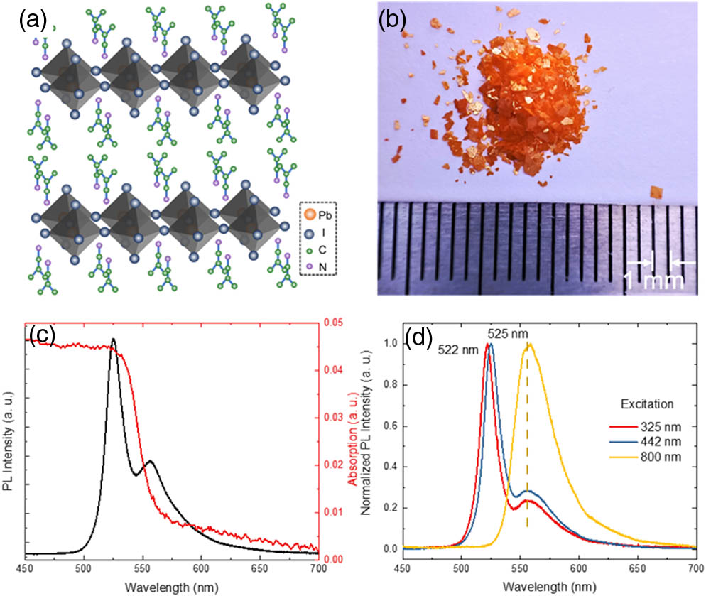
    Figure 1.(a) Schematic crystal structure of (isoBA)2PbI4 crystals. (b) Photograph of as-synthesized (isoBA)2PbI4 crystals. (c) Room-temperature absorption and PL spectra of (isoBA)2PbI4 crystals. (d) PL spectra of (isoBA)2PbI4 crystals under different excitation wavelengths.

    To further confirm the origin of the two emissions, a power-dependent PL measurement at low temperature (40 K) was performed. The PL spectra of (isoBA)2PbI4 single crystals under different excitation powers (0.01–1.00 mW) are shown in Fig. 2(a). With the increase in excitation power, the intensity of the high-energy emission peak increases faster than that of the low-energy one, as shown in the inset of Fig. 2(a). Furthermore, a gradual blueshift of the high-energy emission peak with an increase in excitation power can be found, while the low-energy emission peak is slightly redshifted. These phenomena are related to the laser thermal effect under excitation of a 325 nm laser due to the high photon energy. However, when the excitation source was replaced by a 442 nm laser, the peak positions and relative intensities of the two emissions remained unchanged. The laser thermal effect can be further proved by the following temperature-dependent PL measurement where the emission peak position and relative intensity change under the 325 nm laser excitation. The integrated PL intensities of the two emission peaks under different excitation powers were extracted and are shown in Fig. 2(b). The intensity of the emission peak for high-energy emission shows a linear relationship with excitation power, which confirms the emission is from the recombination of FEs [40]. In contrast, a sub-linear relationship between the intensity of the low-energy emission peak and excitation power is observed. It is known that the integrated intensity of biexciton emission is usually proportional to the square of the excitation power [39]; therefore, the possibility that the low-energy side emission peak originates from biexciton emission can be ruled out. The two-photon excitation emission spectra at room temperature are shown in Fig. 2(c). There is only one emission peak for all excitation powers. The peak position is the same as the low-energy emission of single-photon excitation emission (560 nm), and the integrated intensity of the emissions is proportional to the square of the excitation power. Generally, the thermal effect of 800 nm laser excitation is negligible, and the square linear relationship further eliminates the possibility of biexcitons and defects. Considering a deeper penetration depth for 800 nm laser excitation, it is speculated that this peak originates from STEs that appear inside the material. Therefore, the high-energy side emission peak and low-energy side emission peak are ascribed to FEs and STEs, respectively.

    (a) Low temperature PL emission of (iso−BA)2PbI4 crystals under different excitation intensities. The inset shows normalized spectra. (b) Integrated PL intensity of two emission peaks under different excitation powers. (c) Low temperature PL emission of (iso−BA)2PbI4 crystals under different excitation intensities. The inset shows normalized spectra. (d) Integrated PL intensity of two emission peaks under different excitation powers.

    Figure 2.(a) Low temperature PL emission of (isoBA)2PbI4 crystals under different excitation intensities. The inset shows normalized spectra. (b) Integrated PL intensity of two emission peaks under different excitation powers. (c) Low temperature PL emission of (isoBA)2PbI4 crystals under different excitation intensities. The inset shows normalized spectra. (d) Integrated PL intensity of two emission peaks under different excitation powers.

    Figure 3 plots the temperature-dependent PL spectra excited by a 325 nm laser with a power excitation of 0.5 mW. Both peaks are presented in the whole temperature range from 40 to 300 K, but different temperature dependences can be clearly observed. It can be seen from Fig. 4(a) that the FE peaks slightly blueshift with increasing temperature, while the STE emissions show a significant redshift. With the increase in temperature, the full width at half maximum (FWHM) of the two peaks gradually increases, and the broadening of STEs becomes more obvious. The relative ratio of the integrated PL intensity from two emissions (IEF/ISTE) first increases and then decreases with temperature. These changes are consistent with the observation in Fig. 2, which further confirms the existence of a laser thermal effect. In addition, based on different trends from the temperature-dependent PL spectra, the low-energy emission is excluded to be related to reabsorption.

    (a) Normalized temperature dependent PL spectra from 40 to 300 K. (b) Peak positions of FEs and STEs as a function of temperature. The solid lines are the fitting curves with Eq. (1) described in text. (c) FWHM of FEs and STEs as a function of temperature. The solid lines are the fitting curves with Eq. (2) described in text.

    Figure 3.(a) Normalized temperature dependent PL spectra from 40 to 300 K. (b) Peak positions of FEs and STEs as a function of temperature. The solid lines are the fitting curves with Eq. (1) described in text. (c) FWHM of FEs and STEs as a function of temperature. The solid lines are the fitting curves with Eq. (2) described in text.

    (a) Integrated PL intensity (normalized) of samples at different temperatures. The solid lines are the fitting curves with Eq. (3). The inset shows the ratio of integrated PL intensity of two emissions (IEF/ISTE) at different temperatures. (b) Schematic energy level structure. GS, ground state; FE, free exciton state; FC, free carrier state; STE, self-trapped exciton state; Eg, band energy; Ef−s, trapping barrier energy; Es−f, detrapping barrier energy; Ed, lattice deformation energy.

    Figure 4.(a) Integrated PL intensity (normalized) of samples at different temperatures. The solid lines are the fitting curves with Eq. (3). The inset shows the ratio of integrated PL intensity of two emissions (IEF/ISTE) at different temperatures. (b) Schematic energy level structure. GS, ground state; FE, free exciton state; FC, free carrier state; STE, self-trapped exciton state; Eg, band energy; Efs, trapping barrier energy; Esf, detrapping barrier energy; Ed, lattice deformation energy.

    To further study the emission characteristics of (isoBA)2PbI4 single crystals, the peak positions of FEs and STEs as a function of temperature are plotted in Fig. 3(a). With the increase in temperature, the emission of FEs was slightly blueshifted, while the STEs’ emission redshifted significantly. In perovskite materials, with a temperature increase, the blueshift is usually related to the thermal expansion of a lattice, while the redshift is caused by the electron–phonon interaction [38,41,42]. To better describe the experimental peak positions, both effects should be taken into consideration. The formula is represented as [43] Eg(T)=E0+ATETSω(cothω2kBT1).

    Here, E0 represents the bandgap at 0 K, ATE is the adjustable linear parameter accounting for the contribution of thermal expansion, S is the dimensionless Huang–Rhys (H-R) factor characterizing the electron–photon coupling strength, and ω is the average or effective phonon energy. The black and red curves in Fig. 3(b) are the fitting for FEs and STEs, respectively. For FEs, E0=2.355  eV, ATE=0.058  meV/K, S=0.04, and ω=22.42  meV (R2=0.98528). For STEs, E0=2.322  eV, ATE=0.180  meV/K, S=7.09, and ω=38.21  meV (R2=0.99917). It can be seen that the STE peaks have much higher ATE and S values. The former describes the contribution of thermal expansion, which arises from the anharmonicity of the inter-atomic potentials. Therefore, the bigger values imply that the anharmonicity of self-trapped energy levels is much larger than that of FEs, which is consistent with previous reports [44,45]. The larger S value is also consistent with the stronger electron–phonon interaction required to form STEs [46]. The different average phonon energy may be related to the different locations of excitons in the material.

    The FWHMs of those two peaks were calculated from Fig. 3(a), and the result is shown as a function of temperature in Fig. 3(c). The PL spectra of these two peaks both demonstrate continuous thermal broadening behavior, and the broadening rate for STEs is much higher than that of FEs. Besides the PL peak position, the PL linewidth also carries important information of the electron–phonon interaction. Generally, both homogeneous and inhomogeneous broadenings contribute to the broadening of the emission. The emission broadening with temperature can be fitted according to the following formula [43]: Γ(T)=Γ0+γacT+γLOeωLO/kBT1,where the first term Γ0 represents the temperature-independent inhomogeneous broadening, which arises from the scattering due to the energetic disorders or imperfections. The second and final terms are the homogeneous broadening terms, resulting from the acoustic and longitudinal optical (LO) photon scattering with coupling strengths of γac and γLO, respectively. The black solid line in Fig. 3(c) represents the fitting curve of FE emission, when the parameters Γ0=3.57  meV, γac=0.13  meV/K, γLO=0.45  eV, and ωLO=80.82  meV were adopted. The red solid line represents the fitting curve of STE emission, and the parameters are Γ0=6.19meV, γac=0.24  meV/K, γLO=10.36  eV, and ωLO=114.24  meV. The γac parameter of STEs is larger than that of FEs, which suggests that a strong thermal effect of acoustic photon scattering exists in FE emission. The γLO value for STEs is almost 25 times larger than that of FEs, implying the stronger interaction between excitons and LO phonons. These results indicate that both acoustic and LO phonon scatterings play an important role in the PL broadening of STE emission. It is noted that the fitting curve slightly deviates from the experimental results at temperatures below 80 K, which may be due to the reduced H-R factor of the STEs within this low temperature range.

    Figure 4(a) shows the normalized integrated PL intensity of FEs and STEs at different temperatures. It can be seen that with the increase in temperature, the FE emission intensity first increases and then decreases, while the intensity of the STE emission decreases monotonously. The difference indicates that carrier migration takes place between the two energy states. The band structure was proposed and is schematically shown in Fig. 4(b). In this model, the migration of carriers from FE to STE states needs to overcome the trapping barrier Efs, while the diffusion of carriers from STE into FE states needs to overcome the detrapping barrier Esf. For more detailed interpretation, the model proposed by Poescu et al. [47,48] was used to describe the data:RrNDGe={1+K01+exp(EbkT)[1+i=1Kiexp(EikT)]}1(i=1  or  2),where Rr is the recombination rate of electron–hole pairs, ND is the population of electrons, Ge is the number of carriers captured by the trapping states per unit time, K0 is a constant, k is the Boltzmann constant, T represents temperature, and Eb shows the potential of the barrier. With the increase in temperature, thermally escaped carriers should be considered, where i is the number of thermal escape channels for carriers, Ki is a constant, and Ei represents thermal activation energy. The experimental data of FEs could be perfectly fitted when two thermal escape channels are considered. In this case, Eb represents the detrapping barrier (Esf), E1 represents the trapping barrier (Efs), and E2 can be ascribed to thermally activated nonradiative defects. The values of the potential barriers of detrapping Esf and trapping Efs are estimated to be 18.99 and 10.69 meV, respectively, while E2 is 145.21 meV. Moreover, the integrated PL intensity of STE emission can also be fitted with this formula. At this time, Eb=11.33  meV represents the trapping barrier (Efs), E1=18.16  meV represents the detrapping barrier (Esf), and E2=252.88  meV is also considered as the thermally activated nonradiative defects. By fitting these two curves, it was found that the trapping energy in the band structure model is about 11 meV, and the detrapping energy is about 19 meV. Due to the relatively small trapping barrier, the carriers in FE states have enough energy to overcome the trapping barrier and enter STE states. However, only when the carriers in STE states obtain enough thermal energy from the environment can they overcome the barrier and enter FE states. Moreover, the larger thermally activated nonradiative defect energy in STE emission indicates that STE emission has better temperature stability, which makes it more suitable for optoelectronic devices.

    Next, the reason why only one STE emission peak is observed in the two-photon excitation emission will be discussed. The penetration depth of an 800 nm laser in the material is much larger than that of a 442 nm laser, and therefore, it is speculated that STE emission exists only inside the material. To verify this hypothesis, a microscope fluorescent system was used to measure the sample, and the data are shown in Fig. 5(a). By adjusting the distance between the objective lens and the material surface, the laser focus plane can be adjusted outside, on the surface, or inside the material. After normalizing the spectral intensity according to FEs, it was found that the STE emission shows higher intensity when the focus plane is inside the material, which indicates that STEs appear inside the material. Although there are complicated reasons for the formation of STEs, in 2D perovskites, it is generally related to the deformation of the octahedron [16,25,49]. It is speculated that most of the octahedral deformation in the 2D layered perovskite material occurs inside the material. In this case, there will be no STE emission in a sufficiently thin 2D perovskite material. To verify this claim, (isoBA)2PbI4 thin layers with different thicknesses were prepared. The thickness of the samples is determined by the change of color from the optical image and the focal length of the lens during measurement. It should be noted that the thickness determination is not quantitative. However, it will not influence the discussion about the physical mechanism for the thickness-dependent optical measurement. As shown in Fig. 5(c), the thicknesses of samples 1–4 gradually increase due to the light reflection of the thin film. The 800 nm laser was used to excite these samples, and the PL spectra are shown in Fig. 5(d). It can be clearly seen that the peak position moves from the FE positions to the STEs with the increase in sample thickness. The experimental results are consistent with the model, which implies that the STEs in the 2D perovskite are caused by the octahedral deformation, and mainly exist inside the material. Since the stress on the surface of the material is easier to release, it is not easy to form STEs on the surface of the material. Therefore, the optical properties of STEs in 2D perovskite are related with the octahedral distortion caused by strong electron–phonon interaction inside the materials.

    (a) Microscope PL with different distances between objective lens and material surface. The inset shows PL photos of the sample in light and dark fields. (b) Schematic microscopy fluorescent system. (c) Optical photos of samples with different thicknesses; red arrow indicates the position of laser excitation. The thicknesses of samples 1–4 gradually increase. (d) PL spectra of samples with different sample thicknesses.

    Figure 5.(a) Microscope PL with different distances between objective lens and material surface. The inset shows PL photos of the sample in light and dark fields. (b) Schematic microscopy fluorescent system. (c) Optical photos of samples with different thicknesses; red arrow indicates the position of laser excitation. The thicknesses of samples 1–4 gradually increase. (d) PL spectra of samples with different sample thicknesses.

    Since STEs appear inside the material and propagate along the edge of the material, the relative intensity of the two emission peaks can be used to determine the relative position of the excitation spot on the sample. As shown in Fig. 6, when the 442 nm laser is irradiated on the edge of the material, the relative intensity of STE emission will become larger, and when the laser is irradiated at the center of the material, the relative intensity of STEs will decrease. This kind of optical position sensing is only one of the proof-of-concept demonstrations for applications. Using the relationship between STE emission and material thickness, 2D perovskite materials can be used to make three-dimensional optical storage or information encryption, and the characteristics of multiphoton absorption PL can also be used for multiphoton imaging.

    (a) Relative integrated intensity (IEF/ISTE) of two PL peaks at different positions of the same sample. The inset shows normalized spectra. (b) Excitation spot at different positions of the same sample.

    Figure 6.(a) Relative integrated intensity (IEF/ISTE) of two PL peaks at different positions of the same sample. The inset shows normalized spectra. (b) Excitation spot at different positions of the same sample.

    4. CONCLUSION

    In summary, we have investigated the optical properties of STEs in 2D (isoBA)2PbI4 perovskite crystals, and discussed the reasons for their formation. Temperature-dependent and power-dependent PL measurements were carried out, and results indicate that STEs are related to the octahedral deformation caused by the strong electron–phonon interaction. Trapping and detrapping between STEs and FEs are clearly observed during the temperature-dependent PL measurement. When STEs and FEs obtain enough energy through the surrounding environment, they can overcome the potential barrier and migrate to each other. The characterization of thickness-dependent and two-photon excitation emission further demonstrated the properties of STEs. It is found that STEs usually exist inside the material. Finally, according to these characteristics, potential applications of STEs in 2D perovskite for position sensing and three-dimensional information storage were discussed. This work not only demonstrates the characteristics of STEs but also reveals the reason for the formation of STEs, which will lay the foundation for the application of 2D perovskite materials in the field of optoelectronic devices.

    References

    [1] Y. Chen, Y. Sun, J. Peng, J. Tang, K. Zheng, Z. Liang. 2D Ruddlesden-Popper perovskites for optoelectronics. Adv. Mater., 30, 1703487(2018).

    [2] G. Grancini, M. K. Nazeeruddin. Dimensional tailoring of hybrid perovskites for photovoltaics. Nat. Rev. Mater., 4, 4-22(2018).

    [3] C. Katan, N. Mercier, J. Even. Quantum and dielectric confinement effects in lower-dimensional hybrid perovskite semiconductors. Chem. Rev., 119, 3140-3192(2019).

    [4] B. Zhou, L. Liang, J. Ma, J. Li, W. Li, Z. Liu, H. Li, R. Chen, D. Li. Thermally assisted Rashba splitting and circular photogalvanic effect in aqueously synthesized 2D Dion-Jacobson perovskite crystals. Nano Lett., 21, 4584-4591(2021).

    [5] J. Yu, J. Kong, W. Hao, X. Guo, H. He, W. R. Leow, Z. Liu, P. Cai, G. Qian, S. Li, X. Chen, X. Chen. Broadband extrinsic self-trapped exciton emission in Sn-doped 2D lead-halide perovskites. Adv. Mater., 31, 1806385(2019).

    [6] Z. Guo, X. Wu, T. Zhu, X. Zhu, L. Huang. Electron-phonon scattering in atomically thin 2D perovskites. ACS Nano, 10, 9992-9998(2016).

    [7] Y. Chen, Y. Sun, J. Peng, W. Zhang, X. Su, K. Zheng, T. Pullerits, Z. Liang. Tailoring organic cation of 2D air-stable organometal halide perovskites for highly efficient planar solar cells. Adv. Energy Mater., 7, 1700162(2017).

    [8] L. Mao, Y. Wu, C. C. Stoumpos, M. R. Wasielewski, M. G. Kanatzidis. White-light emission and structural distortion in new corrugated two-dimensional lead bromide perovskites. J. Am. Chem. Soc., 139, 5210-5215(2017).

    [9] C. Quarti, N. Marchal, D. Beljonne. Tuning the optoelectronic properties of two-dimensional hybrid perovskite semiconductors with alkyl chain spacers. J. Phys. Chem. Lett., 9, 3416-3424(2018).

    [10] K. Zheng, Y. Chen, Y. Sun, J. Chen, P. Chábera, R. Schaller, M. J. Al-Marri, S. E. Canton, Z. Liang, T. Pullerits. Inter-phase charge and energy transfer in Ruddlesden-Popper 2D perovskites: critical role of the spacing cations. J. Mater. Chem. A, 6, 6244-6250(2018).

    [11] R. Gautier, M. Paris, F. Massuyeau. Exciton self-trapping in hybrid lead halides: role of halogen. J. Am. Chem. Soc., 141, 12619-12623(2019).

    [12] M. D. Smith, B. A. Connor, H. I. Karunadasa. Tuning the luminescence of layered halide perovskites. Chem. Rev., 119, 3104-3139(2019).

    [13] T. Hu, M. D. Smith, E. R. Dohner, M. J. Sher, X. Wu, M. T. Trinh, A. Fisher, J. Corbett, X. Y. Zhu, H. I. Karunadasa, A. M. Lindenberg. Mechanism for broadband white-light emission from two-dimensional (110) hybrid perovskites. J. Phys. Chem. Lett., 7, 2258-2263(2016).

    [14] J. Luo, X. Wang, S. Li, J. Liu, Y. Guo, G. Niu, L. Yao, Y. Fu, L. Gao, Q. Dong, C. Zhao, M. Leng, F. Ma, W. Liang, L. Wang, S. Jin, J. Han, L. Zhang, J. Etheridge, J. Wang, Y. Yan, E. H. Sargent, J. Tang. Efficient and stable emission of warm-white light from lead-free halide double perovskites. Nature, 563, 541-545(2018).

    [15] O. Nazarenko, M. R. Kotyrba, S. Yakunin, M. Aebli, G. Raino, B. M. Benin, M. Worle, M. V. Kovalenko. Guanidinium-formamidinium lead iodide: a layered perovskite-related compound with red luminescence at room temperature. J. Am. Chem. Soc., 140, 3850-3853(2018).

    [16] S. Wang, Y. Yao, J. Kong, S. Zhao, Z. Sun, Z. Wu, L. Li, J. Luo. Highly efficient white-light emission in a polar two-dimensional hybrid perovskite. Chem. Commun., 54, 4053-4056(2018).

    [17] L. Chao, Z. Wang, Y. Xia, Y. Chen, W. Huang. Recent progress on low dimensional perovskite solar cells. J. Energy Chem., 27, 1091-1100(2018).

    [18] C. Ma, D. Shen, T. W. Ng, M. F. Lo, S. Lee. 2D perovskites with short interlayer distance for high-performance solar cell application. Adv. Mater., 30, 1800710(2018).

    [19] G. Xing, N. Mathews, S. S. Lim, N. Yantara, X. Liu, D. Sabba, M. Grätzel, S. Mhaisalkar, T. C. Sum. Low-temperature solution-processed wavelength-tunable perovskites for lasing. Nat. Mater., 13, 476-480(2014).

    [20] J. Guo, T. Liu, M. Liu, C. Liang, K. Wang, G. Hong, Y. Tang, G. Long, S.-F. Yu, T.-W. Lee, W. Huang, G. Xing. Ultrashort laser pulse doubling by metal-halide perovskite multiple quantum wells. Nat. Commun., 11, 3361(2020).

    [21] Z. Chen, Y. Guo, E. Wertz, J. Shi. Merits and challenges of Ruddlesden-Popper soft halide perovskites in electro-optics and optoelectronics. Adv. Mater., 31, 1803514(2019).

    [22] J. Li, J. Wang, J. Ma, H. Shen, L. Li, X. Duan, D. Li. Self-trapped state enabled filterless narrowband photodetections in 2D layered perovskite single crystals. Nat. Commun., 10, 806(2019).

    [23] L. Li, L. Jin, Y. Zhou, J. Li, J. Ma, S. Wang, W. Li, D. Li. Filterless polarization‐sensitive 2D perovskite narrowband photodetectors. Adv. Opt. Mater., 7, 1900988(2019).

    [24] X. Wu, M. T. Trinh, D. Niesner, H. Zhu, Z. Norman, J. S. Owen, O. Yaffe, B. J. Kudisch, X. Y. Zhu. Trap states in lead iodide perovskites. J. Am. Chem. Soc., 137, 2089-2096(2015).

    [25] J. Li, H. Wang, D. Li. Self-trapped excitons in two-dimensional perovskites. Front. Optoelectron., 13, 225-234(2020).

    [26] W. B. Fowler, M. J. Marrone, M. N. Kabler. Theory of self-trapped exciton luminescence in halide crystals. Phys. Rev. B, 8, 5909-5919(1973).

    [27] R. T. Williams, K. S. Song, W. L. Faust, C. H. Leung. Off-center self-trapped excitons and creation of lattice defects in alkali halide crystals. Phys. Rev. B, 33, 7232-7240(1986).

    [28] D. Menzel. Valence and core excitations in rare gas mono- and multilayers: production, decay, and desorption of neutrals and ions. Appl. Phys. A, 51, 163-171(1990).

    [29] C. Itoh, K. Tanimura, N. Itoh. Optical studies of self-trapped excitons in SiO2. J. Phys. C, 21, 4693-4702(1988).

    [30] S. Yamaoka, Y. Furukawa, M. Nakayama. Initial process of photoluminescence dynamics of self-trapped excitons in a β-Ga2O3 single crystal. Phys. Rev. B, 95, 094304(2017).

    [31] R. Scholz, A. Y. Kobitski, D. R. T. Zahn, M. Schreiber. Investigation of molecular dimers in α-PTCDA by ab initio methods: binding energies, gas-to-crystal shift, and self-trapped excitons. Phys. Rev. B, 72, 245208(2005).

    [32] K. M. McCall, C. C. Stoumpos, S. S. Kostina, M. G. Kanatzidis, B. W. Wessels. Strong electron-phonon coupling and self-trapped excitons in the defect halide perovskites A3M2I9 (A = Cs, Rb; M = Bi, Sb). Chem. Mater., 29, 4129-4145(2017).

    [33] S. Li, J. Luo, J. Liu, J. Tang. Self-trapped excitons in all-inorganic halide perovskites: fundamentals, status, and potential applications. J. Phys. Chem. Lett., 10, 1999-2007(2019).

    [34] T. Li, X. Chen, X. Wang, H. Lu, Y. Yan, M. C. Beard, D. B. Mitzi. Origin of broad-band emission and impact of structural dimensionality in tin-alloyed Ruddlesden-Popper hybrid lead iodide perovskites. ACS Energy Lett., 5, 347-352(2019).

    [35] S.-T. Ha, C. Shen, J. Zhang, Q. Xiong. Laser cooling of organic-inorganic lead halide perovskites. Nat. Photonics, 10, 115-121(2015).

    [36] X. Ma, F. Pan, H. Li, P. Shen, C. Ma, L. Zhang, H. Niu, Y. Zhu, S. Xu, H. Ye. Mechanism of single-photon upconversion photoluminescence in all-inorganic perovskite nanocrystals: the role of self-trapped excitons. J. Phys. Chem. Lett., 10, 5989-5996(2019).

    [37] Y. Liang, Q. Shang, Q. Wi, L. Zhao, Z. Liu, J. Shi, Y. Zhong, J. Chen, Y. Gao, M. Li, X. Liu, G. Xing, Q. Zhang. Lasing from mechanically exfoliated 2D homologous Ruddlesden–Popper perovskite engineered by inorganic layer thickness. Adv. Mater., 31, 1903030(2019).

    [38] S. Wang, J. Ma, W. Li, J. Wang, H. Wang, H. Shen, J. Li, J. Wang, H. Luo, D. Li. Temperature-dependent band gap in two-dimensional perovskites: thermal expansion interaction and electron-phonon interaction. J. Phys. Chem. Lett., 10, 2546-2553(2019).

    [39] W. Li, J. Ma, H. Wang, C. Fang, H. Luo, D. Li. Biexcitons in 2D (iso-BA)2PbI4 perovskite crystals. Nanophotonics, 9, 2001-2006(2020).

    [40] T. Schmidt, K. Lischka, W. Zulehner. Excitation-power dependence of the near-band-edge photoluminescence of semiconductors. Phys. Rev. B, 45, 8989-8994(1992).

    [41] B. Ai, C. Liu, Z. Deng, J. Wang, J. Han, X. Zhao. Low temperature photoluminescence properties of CsPbBr3 quantum dots embedded in glasses. Phys. Chem. Chem. Phys., 19, 17349-17355(2017).

    [42] X. Y. Zhang, G. T. Pang, G. C. Xing, R. Chen. Temperature dependent optical characteristics of all-inorganic CsPbBr3 nanocrystals film. Mater. Today Phys., 15, 100259(2020).

    [43] X. Lao, W. Zhou, Y. Bao, X. Wang, Z. Yang, M. Wang, S. Xu. Photoluminescence signatures of thermal expansion, electron-phonon coupling and phase transitions in cesium lead bromide perovskite nanosheets. Nanoscale, 12, 7315-7320(2020).

    [44] M. A. Collins, D. P. Craig. A model of localization, soliton propagation, and self-trapping in an electronically excited atomic lattice. Chem. Phys., 75, 191-214(1983).

    [45] K. Tanimura, N. Itoh. The hopping motion of the self-trapped exciton in NaCl. J. Phys. Chem. Solid, 42, 901-910(1981).

    [46] R. Leonlli, J. L. Brebner. Time-resolved spectroscopy of the visible emission band in strontium titanate. Phys. Rev. B, 33, 8649-8656(1986).

    [47] P. G. E. Dan Popescu, A. Stintz, K. J. Malloy. Temperature dependence of the photoluminescence emission from InAs quantum dots in a strained Ga0.85In0.15As quantum well. Semicond. Sci. Technol., 19, 33-38(2003).

    [48] R. Chen, H. Y. Liu, H. D. Sun. Electronic energy levels and carrier dynamics in InAs/InGaAs dots-in-a-well structure investigated by optical spectroscopy. J. Appl. Phys., 107, 013513(2010).

    [49] Z. G. Yu. Optical deformation potential and self-trapped excitons in 2D hybrid perovskites. Phys. Chem. Chem. Phys., 21, 22293-22301(2019).

    Haolin Li, Xuanyu Zhang, Haizhen Wang, Jiahao Yu, Kexue Li, Zhipeng Wei, Dehui Li, Rui Chen. Optical characteristics of self-trapped excitons in 2D (iso-BA)2PbI4 perovskite crystals[J]. Photonics Research, 2022, 10(2): 594
    Download Citation