• Journal of Semiconductors
  • Vol. 42, Issue 8, 082001 (2021)
Ankush Parmar1, Jashangeet Kaur2, Manish Dev Sharma1, and Navdeep Goyal1
Author Affiliations
  • 1Centre of Applied Sciences, Department of Physics, Sector-14, Panjab University, Chandigarh 160014, India
  • 2Department of Physics, G.G.D.S.D College, Sector-32, Chandigarh 160030, India
  • show less
    DOI: 10.1088/1674-4926/42/8/082001 Cite this Article
    Ankush Parmar, Jashangeet Kaur, Manish Dev Sharma, Navdeep Goyal. Extensive study of optical contrast between bulk and nanoscale transition metal dichalcogenide semiconductors[J]. Journal of Semiconductors, 2021, 42(8): 082001 Copy Citation Text show less
    (Color online) Schematic diagram for synthesis of nanosheets and fabrication of thin films.
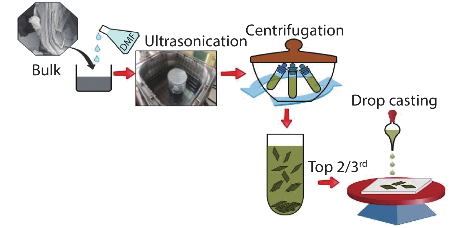
    Fig. 1. (Color online) Schematic diagram for synthesis of nanosheets and fabrication of thin films.
    (Color online) Represents efficient exfoliation of bulk TMDs through (a) XRD spectra of MoS2, (b, c) FESEM of M_bulk and M_exfoliated, and (d) UV–visible spectra of all samples.
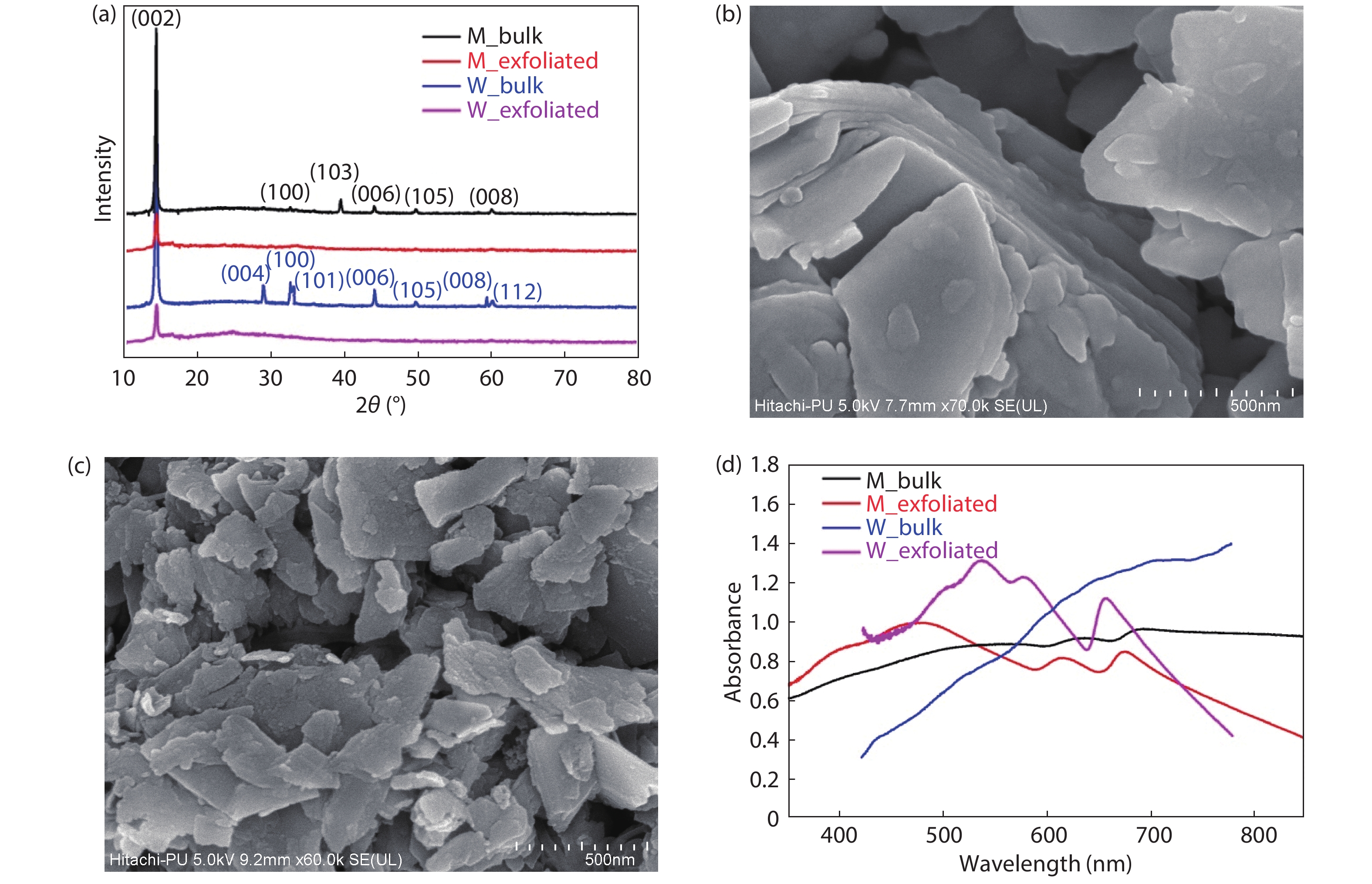
    Fig. 2. (Color online) Represents efficient exfoliation of bulk TMDs through (a) XRD spectra of MoS2, (b, c) FESEM of M_bulk and M_exfoliated, and (d) UV–visible spectra of all samples.
    (Color online) Variation of (a) absorption coefficient, (b) extinction coefficient, and (c) refractive index with incident energy for all the samples.
    Fig. 3. (Color online) Variation of (a) absorption coefficient, (b) extinction coefficient, and (c) refractive index with incident energy for all the samples.
    (Color online) Tauc plot for (a) M_bulk, M_exfoliated and (b) W_bulk, W_exfoliated.
    Fig. 4. (Color online) Tauc plot for (a) M_bulk, M_exfoliated and (b) W_bulk, W_exfoliated.
    (Color online) Variation of (a) real part and (b) imaginary part of dielectric constant with incident energy for all samples. WDM plots for (c) M_bulk, M_exfoliated and (d) W_bulk, W_exfoliated.
    Fig. 5. (Color online) Variation of (a) real part and (b) imaginary part of dielectric constant with incident energy for all samples. WDM plots for (c) M_bulk, M_exfoliated and (d) W_bulk, W_exfoliated.
    SampleEg(opt) (eV) Eu (eV)
    M_bulk1.299.78
    M_exfoliated1.910.57
    W_bulk1.365.31
    W_exfoliated2.000.61
    Table 1. Optical band gap (Eg(opt)) and Urbach energy (Eu) for all the samples.
    SampleEo (eV) Ed (eV) So (10–5) λo (nm) εnoM–1M–3
    M_bulk2.5571.1611.5249.321.0361.01427.914.30
    M_exfoliated4.0591.3324.590.721.0441.02222.551.38
    W_bulk0.9019.921.37944.381.0451.02222.1327.32
    W_exfoliated1.4242.984.05711.041.0331.01630.2715.01
    Table 2. Dispersion energy and oscillator energy parameters for all the samples.
    Ankush Parmar, Jashangeet Kaur, Manish Dev Sharma, Navdeep Goyal. Extensive study of optical contrast between bulk and nanoscale transition metal dichalcogenide semiconductors[J]. Journal of Semiconductors, 2021, 42(8): 082001
    Download Citation