
Ankush Parmar, Jashangeet Kaur, Manish Dev Sharma, Navdeep Goyal. Extensive study of optical contrast between bulk and nanoscale transition metal dichalcogenide semiconductors[J]. Journal of Semiconductors, 2021, 42(8): 082001
- Journal of Semiconductors
- Vol. 42, Issue 8, 082001 (2021)
Abstract
1. Introduction
There has been an outbreak in the study of 2D layered materials since the introduction of graphene. In pursuit of discovering a novel and multi-functional 2D material, TMDs like MoS2, MoSe2, WS2, WSe2 etc. have been investigated by various researchers. They overshadowed the previously recognized graphene, due to their capacious optical absorption and amendable band gaps[
The enhancement in properties of nanosheets as compared to their bulk counterparts can be attributed to the aggravation of the aspect ratio or accessible surface area due to quantum confinement. As we transform the bulk crystals into thin layers, the optical band gap switches from indirect to direct whose absolute value depends upon the layer number. Both the semiconductors have independent benefits, the direct ones find application in light emitting diodes, lasers, solar cells etc. and the indirect ones are suitable for diodes, transistors etc. Therefore, nanoscale TMDs are a potential candidate for solar energy conversion devices and there is an inverse proportionality between the number of layers and extent of optical absorption[
Although we can produce atomically thin nanosheets with the previously mentioned methods, large-scale synthesis remains a challenge. Liquid phase exfoliation surpasses the alternative methods with prominent advantages such as it is affordable, relatively less complex and environment friendly, because of the involvement of organic solvents. The resulting nanosheets are obtained in the form of dispersions which are susceptible to various alterations. For example, they can be processed to form thin films with the help of simple techniques like drop casting[
2. Materials and methods
2.1. Sample preparation
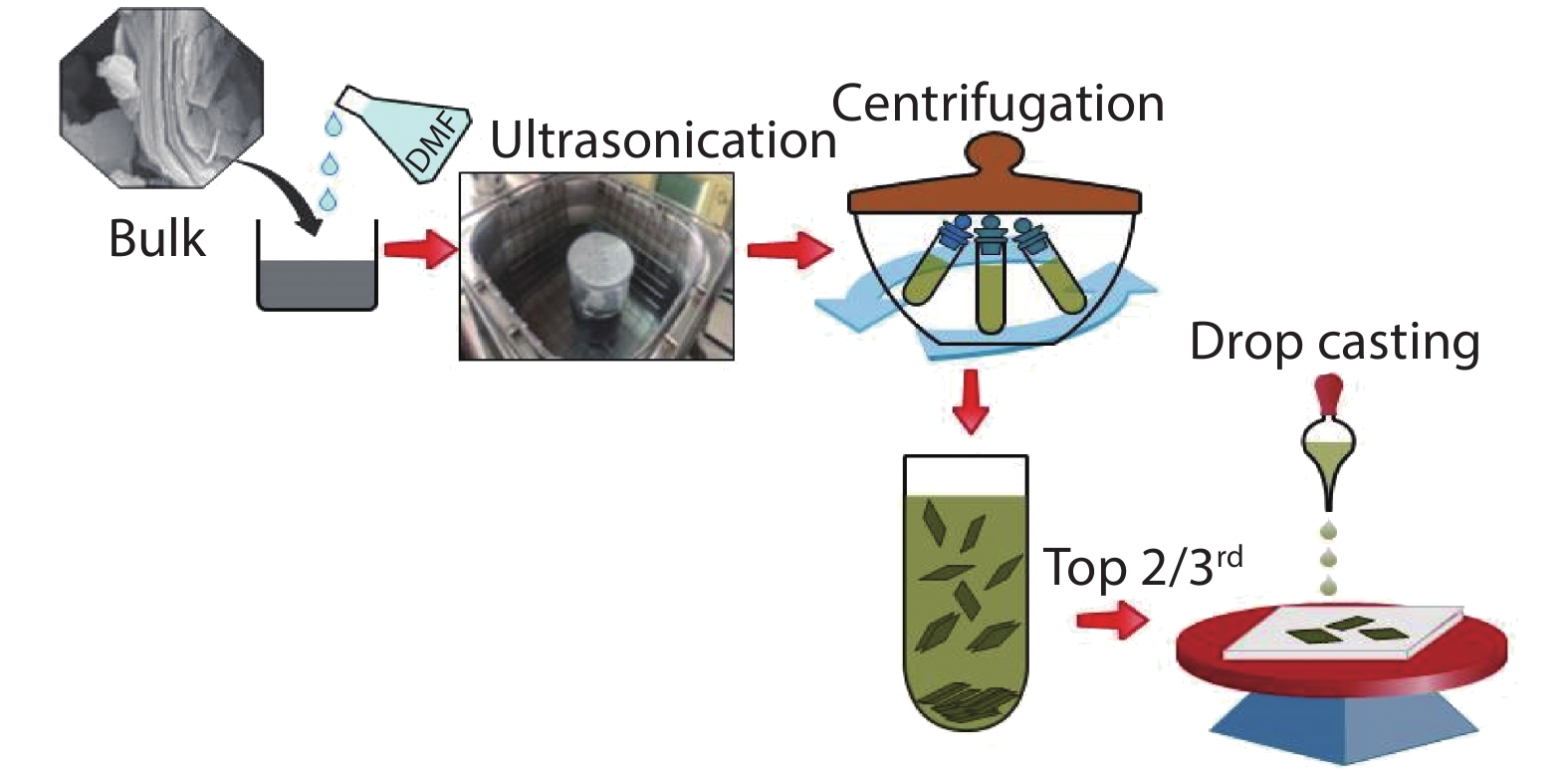
Three-dimensional MoS2 and WS2 bulks were purchased from Sigma Aldrich (CAS no. 1317-33-5 & 12138-09-9 respectively). They were processed and flaked off to yield 2D nanosheets using the liquid exfoliation process (see Fig. 1). 210 mg of bulk powder was added to 30 ml of dimethyl formamide (DMF) in a 50 mL capacity borosil beaker. The dark grey solution was given a mix with spatula for 2–3 min and then covered with parafilm to avoid evaporation. An ultrasonic exfoliation process was carried out in a bath sonicator (Labman Scientific Instruments, 50 W, 40 kHz) for 10 h while maintaining the temperature at 40 °C by regularly circulating water in the bath. The dispersion was then kept undisturbed overnight (approx. 12 h) so that the bulkier particles settle down naturally. A black residue settled at the bottom of the beaker was discarded and the yellowish green solution from top was decanted for centrifugation. The solution was then centrifuged at 10 000 rpm for 30 min. The monolayers or few layer flakes were suspended in the supernatant whereas the precipitate contained heavier nanosheets. The top 2/3rd of supernatant was then pipetted out and drop-casted onto quartz substrates to obtain thin films. The substrates were first ultrasonically cleaned in acetone and then preheated at 60 °C on a hot plate before drop casting. The obtained thin films were used for further characterizations.
![]()
Figure 1.(Color online) Schematic diagram for synthesis of nanosheets and fabrication of thin films.
2.2. Characterizations
For the optical analysis, absorption spectroscopy (Perkin Elmer Lambda-35) in ultraviolet to visible range was carried out. Field emission scanning electron microscopy (FESEM, Hitachi SU 8010) and X-ray diffraction (XRD, PANalytical X’Pert Pro Diffractometer, Cu Kα, λ = 1.24 Å) were performed for the morphology and structural analysis.
3. Theory and calculations
Except from being an economical and simple technique, UV–visible spectroscopy provides a platform to thoroughly understand the optical behavior of a material and its comprehensive analysis. In this work, we have investigated the absorbance spectroscopy of TMDs, by illuminating in the ultraviolet to visible energy range of the electromagnetic spectrum. With the help of the absorbance spectrum, various optical parameters and their variation with the incident energy has been evaluated. The theoretical aspects of this study are described below.
3.1. Optical constants
The capability of a material to absorb the electromagnetic radiation is given by its absorption coefficient which is calculated as:
where A is absorbance and d is the thickness of film.
Similarly, the extinction coefficient can be calculated with the help of absorption coefficient as:
From the reflectance (R) of the material, we can calculate fundamental optical property i.e. refractive index (n)[
Eq. (3) is known as the Fresnel equation which further yields the optical dielectric constants consisting of real and imaginary part. They depend on the values of extinction coefficient and refractive index as follows:
3.2. Optical band gap energy & Urbach energy
Optical transitions take place in a material at a particular energy known as its optical band gap (Eg(opt)). Determining this parameter is vital to describe the transport mechanism and conduction process occurring inside the material. Tauc et al. has given a theory which leads to accurate calculation of Eg(opt) by making use of the Tauc equation which states that[
where n determines whether a semiconductor is direct (n = 2) or indirect (n = 0.5). A Tauc plot is drawn between (αhν)n and hν. The portion of this plot which can be fitted into a straight line is extrapolated to meet the horizontal axis. The point of contact gives the value of Eg(opt). The measure of disorder in a material can be achieved via the Urbach Empirical Rule[
where Eu is the Urbach energy.
Further mathematics yields:
Therefore, a plot of ln(α) vs hν must contain a linear portion whose slope is reciprocal of Urbach Energy (Eu). Eu is a direct measure of extent of order in a material i.e if Eu is higher, then the disorder is more and vice-versa. Some physical parameters for thin films such as optical density and skin depth are also related to the optical constants evaluated above.
3.3. Skin depth, optical density and optical conductivity
Due to morphology, microstructure and varying density of the thin film, the amount of photons penetrating inside the thin film varies with its thickness. This is called the skin effect and the value of thickness at which the number of photons falls to 1/e of its value on the surface of the film, at a particular energy, is known as skin depth (
Another thickness-dependent parameter is optical density (O.D) given as:
The incident photons excite the electrons in the material depending upon their energy. The excited electrons are responsible for conduction and the resultant conductivity is termed as optical conductivity and denoted as σopt. It is related to the optical constants as follows:
where c is the speed of light.
3.4. Dispersion energy parameters
A couple of models have been formulated to evaluate certain optical factors like dispersion energy (Ed), oscillator energy (Eo), oscillator strength (So) and oscillator wavelength (λ0). Eo and Ed are independent parameters which are related to the coordination number of the material and reveals information about the inclusive band configuration. The Wemple Di-Domenico model (WDM) states the dependence of Eo and Ed on refractive index as follows[
This can also be written in the form of a straight line:
Therefore, a graph between (n2–1)–1 and (hν)2 gives the slope as 1/EoEd and intercept as Eo/Ed from which Eo and Ed can be calculated. The static refractive index (n0) and zero frequency dielectric (ε∞) are evaluated by equalizing (hν)2 = 0 in Eq. (13):
Further, Eo and Ed paves way for calculation of moments of spectra M–1 and M–3 as:
Another similar model developed by Sellmeier, known as the Single Sellmeier Model[
Just like the previous model, the plot between (n2–1)–1 and λ–2 has slope = 1/So and intercept 1/(Soλo2). Therefore, we can fetch the values of So and λo from the slope and intercept. These parameters play a decisive role in fabrication and design of opto-electronic spectral devices.
4. Results and discussion
4.1. X-Ray diffraction (XRD)
We have used the XRD study as an initial tool to testify the purity and morphology of our prepared samples. The X-ray patterns of bulk and exfoliated counterparts of both MoS2 and WS2 are shown in Fig. 2(a). In the case of MoS2, the XRD patterns are perfectly comparable with the JCPDS data 03-065-1951, which is indicative of the fact that no impurities were present in the samples. The bulk MoS2 (M_bulk) shows peaks corresponding to (000), (100), (103), (106), (105), (008) out of which the (002) peak is the most intense. In contrast, (002) is the only peak which appears in the XRD of exfoliated MoS2 (M_exfoliated) because exfoliation has occurred along the (002) plane. The prepared nanosheets have retained the crystallinity of its parent material but the stacking number is decreased as the characteristic (002) is broader and less intense in exfoliated material. This is consistent with the findings of other researchers in the past[
![]()
Figure 2.(Color online) Represents efficient exfoliation of bulk TMDs through (a) XRD spectra of MoS2, (b, c) FESEM of M_bulk and M_exfoliated, and (d) UV–visible spectra of all samples.
4.2. Field emission scanning electron microscopy (FESEM)
Both MoS2 and WS2 films were characterized with FESEM to gain further insight into the contrast of lateral dimension and thickness of layers in bulk and exfoliated counterparts of both the materials. The image of M_bulk (Fig. 2(b)) and M_exfoliated (Fig. 2(c)) clearly present a reduction in stacking number and lateral flake dimension by delamination. A similar trend can be seen in WS2 samples shown in Fig. S1 (Supplementary materials).
4.3. UV–visible spectroscopy
As mentioned in the theory, the absorbance of a material can be conversed to evaluate various optical constants, namely absorption coefficient (α), extinction coefficient (k), dielectric constants (εi&εr), refractive index (n) and optical conductivity (σopt) etc. The variation of absorbance with incident wavelength for MoS2 and WS2 are shown in Fig. 2(d). In the case of W_bulk, there is no absorption peak observed but three visible excitonic peaks exist at 462, 521 and 629 nm in the spectra of W_exfoliated.
The absorbance spectra of M_bulk unveil excitonic peaks at 637 and 691 nm, respectively. These peaks are shifted towards decreasing wavelengths in the case of M_exfoliated with peak positions at 616 and 675 nm. This blue shift acknowledges a substantial fragmentation of thick flakes into few-layer nanosheets[
4.3.1. Assessment of optical constants
The potential of an optically active material is determined by its capability of absorption of light, which can be described by evaluation of optical constants like α and k. Using Eqs. (1) and (2), the variation of α and k with incident energy for all the samples are shown in Figs. 3(a) and 3(b). In the case of bulk samples (M_bulk & W_bulk), both α and k decrease with increasing incident energy. However, for M_exfoliated and W_exfoliated, there are augmented values at certain points in the visible region of incident energy which signify maximas of absorption. High absorption at certain energies, make these materials advisable for opto-electronic applications. Further, with the values of k, we calculated the refractive index (n) with the help of Eq. (3). It decreases with incident energy (or increases with incident wavelength) for bulk samples in the whole range of illumination depicting normal behavior of the dispersions (see Fig. 3(c)).
![]()
Figure 3.(Color online) Variation of (a) absorption coefficient, (b) extinction coefficient, and (c) refractive index with incident energy for all the samples.
This is known as a “normal behavior”. On the other hand, refractive index is very sensitive to incident energy in exfoliated samples. In the lower energy region up to 2.5 eV, the dispersions behave anomalously, but in a higher energy range they behave normally[
4.3.2. Determination of optical band gap and Urbach Energy
To determine the optical band gap of a material, the method developed by Tauc was adopted. In the case of our samples, both MoS2 and WS2 clearly unveiled a transformation from indirect band gap semiconductor to a direct band gap semiconductor upon exfoliation (see Fig. 4). The optical band gaps determined for all samples using Eq. (6) are summarized in Table 1. An optical band gap contrast (i.e. the difference between Eg(opt) of bulk and exfoliated samples) of around 0.62 eV and of 0.64 eV has been found in MoS2 and WS2 samples respectively. This reassures that the band gap transitions lying in the UV–visible spectrum are responsible for semiconducting opto-electronic applications of such TMDs. The variation of ln(α) with incident energy is drawn in the low energy range in Fig. S5. The reciprocal of the slope of this graph gives the value of Eu which is calculated and listed in Table 1.
![]()
Figure 4.(Color online) Tauc plot for (a) M_bulk, M_exfoliated and (b) W_bulk, W_exfoliated.
Table Infomation Is Not Enable4.3.3. Dielectric constant
The comprehensive study of dielectric function is the foundation of profound understanding of optical phenomenon occurring in the material when it is excited with photon energy[
![]()
Figure 5.(Color online) Variation of (a) real part and (b) imaginary part of dielectric constant with incident energy for all samples. WDM plots for (c) M_bulk, M_exfoliated and (d) W_bulk, W_exfoliated.
4.3.4. Wemple Di-domenico model (WDM)
The optical analysis of any material that finds applications in the electromagnetic spectral range devices is incomplete without evaluation of dispersion energy and oscillator energy parameters. By using the values of refractive indices in Eq. (13), a variation of (n2–1)–1 vs (hν)2 has been plotted according to WDM (see Figs. 5(c) and 5(d)). The linear portion of the graph gives the values of slopes and intercepts which further yield the WDM parameters. Further, the relationship between (n2–1)–1 vs λ–2 (Fig. S6) yields the SSM parameters using Eq. (17). The parameters are summarized in Table 2. Few more vital parameters were calculated using Eqs. (14)–(16). These are moments of spectra, static referactive index and zero frequency dielectric constant respectively.
5. Conclusion
Extensive optical study has been performed on MoS2 and WS2 TMDs in both bulk and nanomaterial morphologies. The “multilayer” to “few-layer” transformation was achieved with the liquid exfoliation process. The resulting nanosheet dispersions were drop-casted onto quartz substrates for further investigations. Several initial tests like XRD and FESEM were carried out to assure the successful exfoliation. UV–visible spectroscopy served as the major tool to thoroughly examine the optical response of TMDs from ultraviolet to visible range of frequencies. Beginning with the absorbance spectra, various optical constants were calculated and their variation with incident energy has been explained. The data was fitted with WDM and SSM models to evaluate dispersion energy and oscillator energy parameters. The performance statistics of nanosheets have been found to be greatly enhanced as compared to the bulk counterparts. This exclusive analysis is novel to TMDs, as there is no clear distinction between the optical parameters of bulk and nanosheets reported so far, to our knowledge. The spectral variation of optical constants can help in understanding a particular optical phenomenon and makes way for more suitable applications in photonics and electronics. For example, the presence of sharp excitation peaks at certain values of incident energies can be useful in creating excitation wavelengths.
Acknowledgements
We would like to acknowledge SAIF, CIL, Panjab University, Chandigarh, for the characterization facilities and the Department of Physics, Panjab University, Chandigarh, for laboratory equipments.
Appendix A. Supplementary materials
Supplementary materials to this article can be found online at https://doi.org/1674-4926/42/8/082001.
References
[1] X R Gan, H M Zhao, X Quan. Two-dimensional MoS2: A promising building block for biosensors. Biosens Bioelectron, 89, 56(2017).
[2] S Deb, P Chakrabarti, P K Mohapatra et al. Tailoring of defect luminescence in CVD grown monolayer MoS2 film. Appl Surf Sci, 445, 542(2018).
[3] T Sekine, C Julien, I Samaras et al. Vibrational modifications on lithium intercalation in MoS2. Mater Sci Eng B, 3, 153(1989).
[4] A G Kelly, V Vega-Mayoral, J B Boland et al. Whiskey-phase exfoliation: Exfoliation and printing of nanosheets using Irish whiskey. 2D Mater, 6, 045036(2019).
[5] Q Wang, K Kalantar-Zadeh, A Kis et al. Electronics and optoelectronics of two-dimensional transition metal dichalcogenides. Nat Nanotechnol, 7, 699(2012).
[6] S S Ji, Z Yang, C Zhang et al. Exfoliated MoS2 nanosheets as efficient catalysts for electrochemical hydrogen evolution. Electrochimica Acta, 109, 269(2013).
[7] F Tudorache, P D Popa, M Dobromir et al. Studies on the structure and gas sensing properties of nickel-cobalt ferrite thin films prepared by spin coating. Mater Sci Eng B, 178, 1334(2013).
[8] D Vikraman, S Hussain, L Truong et al. Fabrication of MoS2/WSe2 heterostructures as electrocatalyst for enhanced hydrogen evolution reaction. Appl Surf Sci, 480, 611(2019).
[9] C Yim, M O'Brien, N McEvoy et al. Investigation of the optical properties of MoS2 thin films using spectroscopic ellipsometry. Appl Phys Lett, 104, 103114(2014).
[10] A H Reshak, S Auluck. Calculated optical properties of 2H-MoS2 intercalated with lithium. Phys Rev B, 68, 125101(2003).
[11] J Kaur, A Parmar, S K Tripathi et al. Optical Study of Ge1Sb2Te4 and GeSbTe thin films. Mater Res Express, 6, 046417(2019).
[12] N Saha, A Sarkar, A B Ghosh et al. Highly active spherical amorphous MoS2: Facile synthesis and application in photocatalytic degradation of rose Bengal dye and hydrogenation of nitroarenes. RSC Adv, 5, 88848(2015).
[13] S Çabuk, A Mamedov. Urbach rule and optical properties of the LiNbO3 and LiTaO3. J Opt A, 1, 424(1999).
[14] G Galeczki. Wemple-didomenico plots for the refractive index of PbTe. Infrared Phys, 31, 215(1991).
[15] R Jha, S Santra, P K Guha. Green synthesis route for WS2 nanosheets using water intercalation. Mater Res Express, 3, 095014(2016).
[16] X J Tian, J Y Wu, Q Li et al. Scalable production of few-layer molybdenum disulfide nanosheets by supercritical carbon dioxide. J Mater Sci, 53, 7258(2018).
[17] N N Dong, Y X Li, Y Y Feng et al. Optical limiting and theoretical modelling of layered transition metal dichalcogenide nanosheets. Sci Rep, 5, 14646(2015).
[18] S Yasmeen, F Iqbal, T Munawar et al. Synthesis, structural and optical analysis of surfactant assisted ZnO-NiO nanocomposites prepared by homogeneous precipitation method. Ceram Int, 45, 17859(2019).
[19] S S Devangamath, B Lobo. Optical parameters of epoxy-CoSO4·7H2O polymer hybrid material. Mater Res Innov, 24, 152(2020).
[20] J Kaur, A Parmar, S K Tripathi et al. Temperature-dependent opto-electronic properties of Ge2.53Sb4.89Te2.50 thin films. Phase Transitions, 93, 134(2020).

Set citation alerts for the article
Please enter your email address
© Copyright 2018-2021 | Chinese Laser Press. All Rights Reserved 沪ICP备15018463号-20