• Chinese Journal of Quantum Electronics
  • Vol. 40, Issue 3, 369 (2023)
ZHANG Minghao1, DONG Yazhou2, and LIANG Shixiong3,*
Author Affiliations
  • 1Hebei Academy of Product Quality Supervision and Inspection, Shijiazhuang 050000, China
  • 2University of Electronic Science and Technology of China, Chengdu 610000, China
  • 3National Key Laboratory of ASIC, The 13th Research Institute of China Electronics Technology Group Corporation, Shijiazhuang 050000, China
  • show less
    DOI: 10.3969/j.issn.1007-5461.2023.03.008 Cite this Article
    Minghao ZHANG, Yazhou DONG, Shixiong LIANG. 340 GHz transceiver link based on Schottky diode monolithic integrated chip[J]. Chinese Journal of Quantum Electronics, 2023, 40(3): 369 Copy Citation Text show less
    Photo of terahertz Schottky diode chip (a) and monolithic circuit (b)
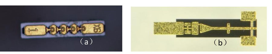
    Fig. 1. Photo of terahertz Schottky diode chip (a) and monolithic circuit (b)
    Schematic diagram of the overall circuit topology of the 340 GHz mixer
    Fig. 2. Schematic diagram of the overall circuit topology of the 340 GHz mixer
    The 340 GHz mixer simulation result. (a) Simulation result of frequency conversion loss;(b) S11 parameter of local oscillator input port; (c) S22 parameter of RF input port
    Fig. 3. The 340 GHz mixer simulation result. (a) Simulation result of frequency conversion loss;(b) S11 parameter of local oscillator input port; (c) S22 parameter of RF input port
    Overall circuit diagram of frequency doubler. (a) Simulation model of three-dimensional electromagnetic field;(b) ADS circuit model in frequency doubler
    Fig. 4. Overall circuit diagram of frequency doubler. (a) Simulation model of three-dimensional electromagnetic field;(b) ADS circuit model in frequency doubler
    Efficiency simulation results of (a) 170 GHz and (b) 340 GHz frequency doubler
    Fig. 5. Efficiency simulation results of (a) 170 GHz and (b) 340 GHz frequency doubler
    Schematic diagram of 340 GHz transmission link
    Fig. 6. Schematic diagram of 340 GHz transmission link
    (a) Output power test curve and (b) photos of 340 GHz frequency doubler lin
    Fig. 7. (a) Output power test curve and (b) photos of 340 GHz frequency doubler lin
    Schematic diagram of the 340 GHz receiving link
    Fig. 8. Schematic diagram of the 340 GHz receiving link
    (a) Conversion loss test result of 340 GHz sub-harmonic mixer; (b) Photos of 340 GHz mixer link
    Fig. 9. (a) Conversion loss test result of 340 GHz sub-harmonic mixer; (b) Photos of 340 GHz mixer link
    Minghao ZHANG, Yazhou DONG, Shixiong LIANG. 340 GHz transceiver link based on Schottky diode monolithic integrated chip[J]. Chinese Journal of Quantum Electronics, 2023, 40(3): 369
    Download Citation