
Zihan Zhao, Yue Wang, Xumin Ding, Haoyu Li, Jiahui Fu, Kuang Zhang, Shah Nawaz Burokur, Qun Wu, "Compact logic operator utilizing a single-layer metasurface," Photonics Res. 10, 316 (2022)
- Photonics Research
- Vol. 10, Issue 2, 316 (2022)
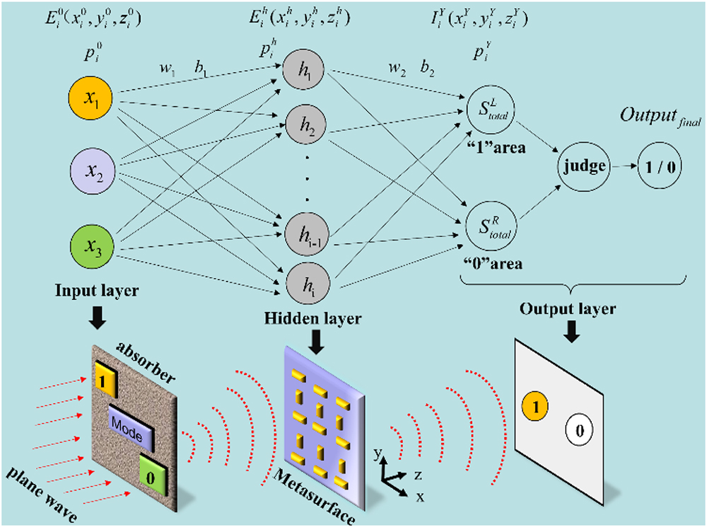
Fig. 1. Input, hidden, and output layers and parameters of the FCNN used in this paper, and the corresponding physical implementations.
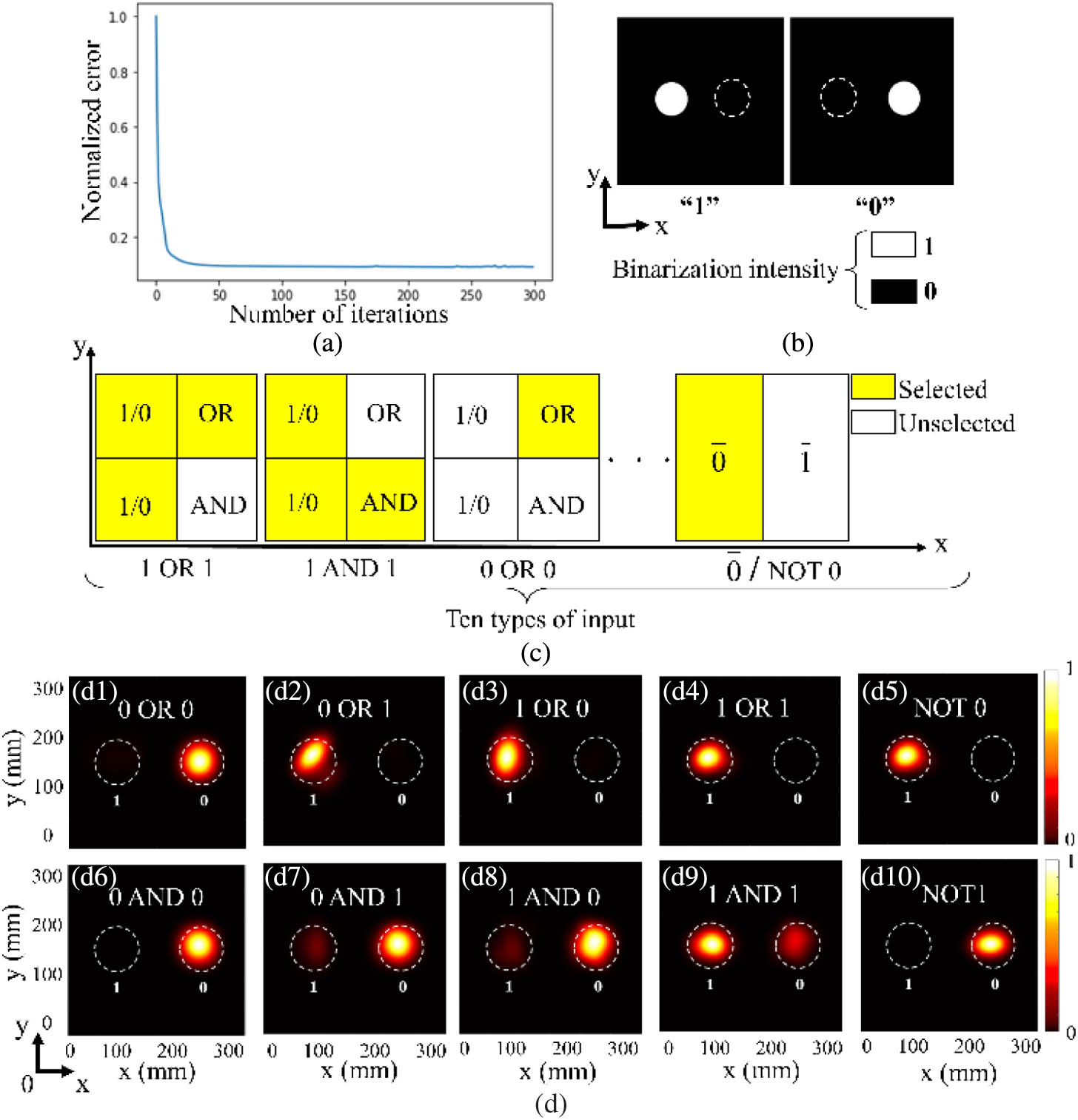
Fig. 2. (a) Curve of the error between the obtained and ideal results during the iteration of FCNN. (b) Designed target output image utilized for training the FCNN. (c) Designed 10 types of input corresponding to all the basic logic operation functions in this paper. (d) Electric field intensity distribution on the output layer when the distance between the hidden and output layers is 10 λ
Fig. 3. (a) Schematic diagram of the unit cell for the proposed single-layer metasurface and corresponding simulation settings. (b) Photograph of the fabricated single-layer metasurface. (c) Phase map of the optimized metasurface-based optical logic operator. (d) Full-wave simulated results of the output electric field intensity distribution for different input logic operations in the observation plane (output layer) located 10 λ
Fig. 4. Schematic diagram of the measured scenario for the optical logic operator. The inset shows the structure of the tailored absorbers performing as the input layer.
Fig. 5. (a) Measured results of input electric field intensity distribution on the proposed metasurface for different logic operations: (a1) 0 OR 0, (a2) 0 OR 1, (a3) 1 OR 0, (a4) 1 OR 1, (a5) NOT 0, (a6) 0 AND 0, (a7) 0 AND 1, (a8) 1 AND 0, (a9) 1 AND 1, and (a10) NOT 1. (b) Measured results of all basic logical operations illustrated by the electric field intensity distribution of the output layer in an observation plane located 10 λ


Set citation alerts for the article
Please enter your email address

© Copyright 2018-2021 | Chinese Laser Press. All Rights Reserved 沪ICP备15018463号-20