
Zihan Zhao, Yue Wang, Xumin Ding, Haoyu Li, Jiahui Fu, Kuang Zhang, Shah Nawaz Burokur, Qun Wu, "Compact logic operator utilizing a single-layer metasurface," Photonics Res. 10, 316 (2022)
- Photonics Research
- Vol. 10, Issue 2, 316 (2022)
Abstract
1. INTRODUCTION
Compared to traditional electronic computing devices [1–3], numerical computing based on optical devices shows the characteristics of parallel processing, ultrahigh-speed, and low power consumption [4–6], which has attracted enormous interests in recent years. As the most basic computing operation, optical logic operation plays a very important role in the field of ultrahigh-speed information transmission and communications [7]. The design and implementation of traditional optical logic computing devices are mostly based on plasmas [8–11], silicon micro-rings (“AND” and “NAND” operations) [12], and a photonic crystal nanocavity [13]. By implementing interference to the input signal, the output signal shows two states with a large difference in intensity, which represent two kinds of logic information: “0” and “1.” However, in previous studies on the design of optical logic operation devices, it was necessary to control the light source precisely (including the intensity and phase difference) to obtain the desired outputs [7]. To generate the expected light source, these devices are often large in size. In addition, due to the high sensitivity to external interference, it is difficult to obtain a significant signal intensity difference that represents logic information in the experimental scenarios [10].
Metasurface, as a new type of artificial electromagnetic material, has simple structure and sub-wavelength thickness [14–23], which avoids the problem of a large volume, which is intrinsic to traditional lens-based optical computing devices and provides the possibility to realize compact optical computing devices [24–30]. With the ability to manipulate the amplitude and phase of the incident wave, the metasurface overcomes the alignment and aberrations problems that result from the features of lenses [26,31]. In previous reported works, metasurfaces have been applied to a variety of optical computing scenarios, such as optical convolution and differentiation [32], Laplacian operation [33], edge extraction [34], and equation solvers [35]. However, these reported metasurface-based optical computing strategies rely on the specific structure of optical metasurface design with complex and high-cost machining processes. At the same time, the fixed structural parameters of unit cells, which cannot be arbitrarily modified during the design and optimization process, also challenge the flexibility of the design. Due to the outstanding design and optimization capabilities, deep learning has attracted much attention in many topics and research fields [36–42]. The superiority of this method has been verified in the optimization work of unit cell structure and array performance [43–49]. Notably, such a method also shows great potential in designing optical operational devices since the artificial neural network can perfectly describe the process of electromagnetic (EM) wave diffraction. Several deep-learning-based optical computational systems using a metasurface are proposed, such as mathematical operations [50–52], target recognition [53–57], image processing [58], cloaking [59], and holographic generation [60,61], to name a few. In addition, optical logic operation also can be realized by combining deep learning and metasurface technology. In this case, plane waves can be chosen as the incident signal, and will be converged to the designated zones in the output layer through the scattering of the metasurface, which can avoid the strict requirements on the light source and bulky optical apparatus. The input (light source) and hidden layer (corresponding metasurface structure) also can be arbitrarily changed to obtain the desired output results by training the network to improve the flexibility of the design. For example, an optical logic operator based on a multilayer dielectric structured metasurface corresponding to a two-layer diffractive neural network has been proposed and experimentally demonstrated to realize basic logic operations [62], which proves the feasibility of this method in the design of an optical logic operator and makes the realization of miniaturized programmable optical processors possible.
In this paper, we design a single-layer metasurface-based compact logic operator using a diffractive neural network. The nodes in the hidden layer of the fully connected neural network (FCNN) can be mapped to the unit cells of the metasurface. When the incident wave illuminates a specific region of the metasurface and the relative logical operation and input value are selected, the transmitted wave will be scattered and focused to specific zones in the output layer with logical information (“1” and “0”). After training the FCNN, three basic logic operation functions (AND, OR, and NOT) are theoretically and experimentally verified with the same metasurface, and the measured results agree very well with the theoretical predictions and simulated results. The proposed metasurface-based logic operator uses subwavelength-thickness strip resonators, which are quite compact and easy to process. In addition, the artificial neural network with only one hidden layer is achieved by using a single-layer metasurface, which provides the possibility to realize compact photonic processors and integrated optical computing systems. More importantly, due to the single-layer network design and optimized functional partition of input and output layers, the resources and time to train the network are greatly reduced.
Sign up for Photonics Research TOC. Get the latest issue of Photonics Research delivered right to you!Sign up now
2. DESIGN OF FCNN AND OPTICAL LOGIC OPERATOR
Since the output results of optical logic operators possess only two states (“1” or “0”) with different input light sources, it is very similar to the classification problem in deep learning architectures [63]. Therefore, the optical logic operator can be constructed based on related machine learning theories. The single-layer FCNN is selected as a design template, since the scattering and propagation characteristics of an EM wave are very similar to such a network. Figure 1 shows the physical models to implement the single-layer FCNN used in this work. The input layer is implemented by appropriately carved absorbers in the microwave band to control the shape of the incident wave, which represents the input value and operation type. The hidden layer is implemented by a single-layer metasurface composed of subwavelength thickness strip resonators, which can modulate the incident wavefront and transfer it to the output layer. Elaborately, the output layer is designed to be two circular areas with logical information (“1” and “0”), and the transmitted wave will be converged to one of them to show the output results. Consequently, the mapping relationship between the FCNN and the metasurface can be achieved. First, in the hidden layer, the Pancharatnam–Berry (PB) phase unit cells that can introduce abrupt phase changes to the incident wave are used to represent the nodes [64]. The value of the nodes in each layer of the FCNN (
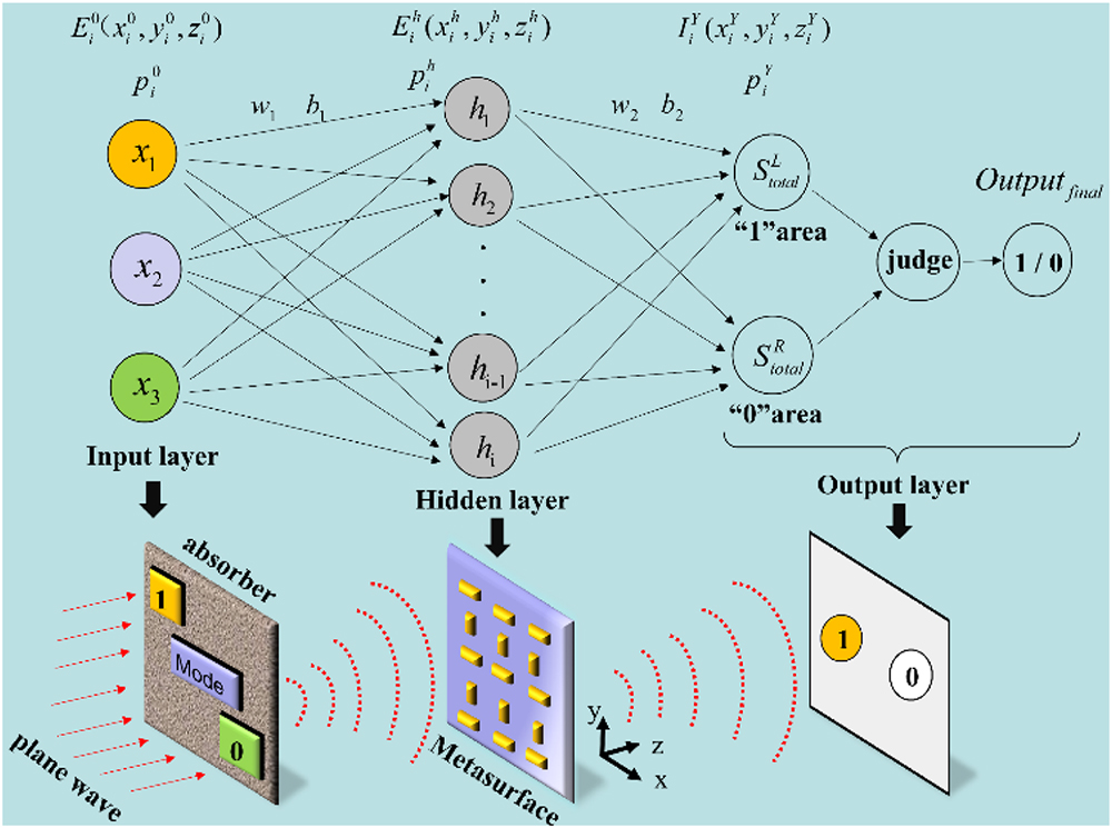
Figure 1.Input, hidden, and output layers and parameters of the FCNN used in this paper, and the corresponding physical implementations.
After the forward propagation through the input and hidden layers, the electric field distribution on the output layer can be described as
Furthermore, the final logic output results can be judged as
Moreover, in this work, the gradient descent method is applied to continuously optimize the phase bias and reduce the loss function until the network converges. As shown in Fig. 2(a), the value of the loss function of the FCNN basically converges after 300 iterations while ensuring good training results. To achieve all basic logic operations, the functional partition of the input layer and the target images of the output layer are elaborately designed, as shown in Figs. 2(b) and 2(c). In the output layer, the size of two focal areas containing logical information and the distance between them have been optimized, which can reduce the loss function when performing iterative operations to save the time to train the network. The functional partition of the input layer is divided into four optional blocks composed of value selections and logical operation areas, and can implement 10 different input operations by applying the regional multiplex strategy. For example, as shown in Fig. 2(c), the input conditions of “OR” and “AND” are independent of each other, while the operation areas of “NOT 1” and “NOT 0” cover two value selection areas and two logic operation areas, respectively. Notably, the inputs of “NOT 1” and “NOT 0” are complementary and do not conflict with the logic operations of “OR” and “AND.” With such a design, the size of the required metasurface is significantly reduced since there are only four optional areas. At the same time, fewer optional areas ensure sufficient size of each functional area and uniformity of the incident wave energy for all logic operations. More importantly, based on the designs mentioned above, all the basic logical operations can be achieved with one hidden layer after optimization, which means that only one piece of metasurface is required for physical implementation, further improving the compactness of the optical logic operator device.
![]()
Figure 2.(a) Curve of the error between the obtained and ideal results during the iteration of FCNN. (b) Designed target output image utilized for training the FCNN. (c) Designed 10 types of input corresponding to all the basic logic operation functions in this paper. (d) Electric field intensity distribution on the output layer when the distance between the hidden and output layers is
After fully training the network based on the target images, the numerical demonstration of the functions of this network is performed and shown in Fig. 2(d). Here, the distance between the output and hidden layers is set to be
3. SIMULATED AND EXPERIMENTAL DEMONSTRATION
For physical implementation, it is important to design a metasurface composed of unit cells that can modify the phase of the incident wave accurately. Here, a metasurface based on the single layer PB phase element illustrated in Fig. 3(a) operates as the hidden layer to manipulate the phase distribution of the transmitted wave through the geometric phase distribution. The unit cell structure is composed of the metal strip with a length of 6.8 mm, a width of 0.5 mm, and a thickness of 0.018 mm, printed on a 2 mm thick dielectric substrate with relative permittivity
![]()
Figure 3.(a) Schematic diagram of the unit cell for the proposed single-layer metasurface and corresponding simulation settings. (b) Photograph of the fabricated single-layer metasurface. (c) Phase map of the optimized metasurface-based optical logic operator. (d) Full-wave simulated results of the output electric field intensity distribution for different input logic operations in the observation plane (output layer) located
After sufficient training, the phase offset of each node in the hidden layer is obtained, which determines the rotation angle of each unit cell of the metasurface. Figure 3(b) shows a photograph of the proposed metasurface construction and Fig. 3(c) demonstrates phase map of the designed metasurface. Compared to the optical logical operator based on 3D printed
![]()
Figure 4.Schematic diagram of the measured scenario for the optical logic operator. The inset shows the structure of the tailored absorbers performing as the input layer.
Here, the horn antenna is placed far enough away (about 50
![]()
Figure 5.(a) Measured results of input electric field intensity distribution on the proposed metasurface for different logic operations: (a1) 0 OR 0, (a2) 0 OR 1, (a3) 1 OR 0, (a4) 1 OR 1, (a5) NOT 0, (a6) 0 AND 0, (a7) 0 AND 1, (a8) 1 AND 0, (a9) 1 AND 1, and (a10) NOT 1. (b) Measured results of all basic logical operations illustrated by the electric field intensity distribution of the output layer in an observation plane located
Furthermore, according to Eqs. (8)–(10), the maximum electric field energy distribution on the output layer for each logic operation is confined in the two designated zones with logic information. Therefore, the logical operation results can be judged intuitively from the electric field energy distribution on the center line passing through the two designated zones. Consequently, the measured results are plotted to obtain the output results of all logic operations, as shown in Fig. 5(c). It can be seen that the peak of the electric field energy along the selected line is well confined in the designated output zone, and the corresponding demonstrated logical results (the horizontal position of the peaks) are consistent with the theoretical values and numerically simulated results. Such a design can be extended to higher frequencies, such as terahertz and optical regimes, through the utilization of nanostructured PB phase elements that may be composed of α-silicon, single crystal silicon, TiO2, and GaN. Moreover, the metasurface array can be optimized by means of inverse design methods [68], such as the inverse design based on a tandem neural network (T-NN) [69], to further miniaturize the optical logic operator.
4. CONCLUSION
In conclusion, by using a diffractive neural network, a compact logic operator based on a single-layer metasurface is proposed at a microwave frequency to realize the three basic logic operations of AND, OR, and NOT. It has been theoretically and experimentally verified that the proposed logic operator can well realize all the designed functions, and the measured results are in good agreement with the theoretical and calculated results. The neural network used in this design has only one hidden layer, which provides remarkable improvements in training speed and computational resource usage. In addition, this optical logic operator is implemented by a single-layer metasurface composed of compact unit cell structures, which means that it is easy to process and integrate with other optical devices. Moreover, the designed method also can be readily applied to other frequency regimes and implementations would be possible with suitable fabrication technologies.
References
[1] A. V. Oppenheim, J. S. Lim, B. R. Musicus, A. B. Baggeroer, M. Feder, G. Aliberti. Digital Signal Processing(1987).
[2] D. R. Solli, B. Jalali. Analog optical computing. Nat. Photonics, 9, 704-706(2015).
[3] J. S. Small. General-purpose electronic analog computing: 1945–1965. IEEE Ann. Hist. Comput., 15, 8-18(1993).
[4] R. Athale, D. Psaltis. Optical computing: past and future. Opt. Photon. News, 27, 32-39(2016).
[5] Y. Zhou, H. Zheng, I. I. Kravchenko, J. Valentine. Flat optics for image differentiation. Nat. Photonics, 14, 316-323(2020).
[6] N. V. Golovastikov, D. A. Bykov, L. L. Doskolovich, E. A. Bezus. Spatial optical integrator based on phase-shifted Bragg gratings. Opt. Commun., 338, 457-460(2015).
[7] D. A. B. Miller. Are optical transistors the logical next step?. Nat. Photonics, 4, 3-5(2010).
[8] H. Wei, Z. P. Li, X. R. Tain, Z. X. Wang, F. Z. Cong, N. Liu, S. P. Zhang, P. Nordlander, N. J. Halas, H. X. Xu. Quantum dot-based local field imaging reveals plasmon-based interferometric logic in silver nanowire networks. Nano Lett., 11, 471-475(2011).
[9] H. Wei, Z. P. Li, X. R. Tain, M. Käll, H. X. Xu. Cascaded logic gates in nanophotonic plasmon networks. Nat. Commun., 2, 387(2011).
[10] Y. L. Fu, X. Y. Hu, C. C. Lu, S. Yue, H. Yang, Q. H. Gong. All-optical logic gates based on nanoscale plasmonic slot waveguides. Nano Lett., 12, 5784-5790(2012).
[11] Y. G. Sang, X. Wu, S. S. Raja, C. Y. Wang, H. Z. Li, Y. F. Ding, D. H. Liu, J. Zhou, H. Ahn, S. Gwo, J. W. Shi. Broadband multifunctional plasmonic logic gates. Adv. Opt. Mater., 6, 1701368(2018).
[12] Q. F. Xu, M. Lipson. All-optical logic based on silicon micro-ring resonators. Opt. Express, 15, 924-929(2007).
[13] M. W. McCutcheon, G. W. Rieger, J. F. Young, D. Dalacu, P. J. Poole, R. L. Williams. All-optical conditional logic with a nonlinear photonic crystal nanocavity. Appl. Phys. Lett., 95, 221102(2009).
[14] N. Yu, F. Capasso. Flat optics with designer metasurfaces. Nat. Mater., 13, 139-150(2014).
[15] Y. Zhao, A. Alù. Manipulating light polarization with ultrathin plasmonic metasurfaces. Phys. Rev. B., 84, 205428(2011).
[16] S. Zahra, L. Ma, W. Wang, J. Li, G. Wen. Electromagnetic metasurfaces and reconfigurable metasurfaces: a review. Front. Phys., 8, 615(2021).
[17] X. M. Ding, Z. C. Wang, S. Y. Liu, K. Zhang, Q. Wu. Polarization-multiplexed Huygens metasurface holography. Opt. Lett., 45, 5488-5491(2020).
[18] C. S. Guan, X. M. Ding, Z. C. Wang, K. Zhang, M. Jin, S. N. Burokur, Q. Wu. Helicity-switched hologram utilizing a polarization-free multi-bit coding metasurface. Opt. Express, 28, 22669-22678(2020).
[19] C. S. Guan, Z. C. Wang, X. M. Ding, K. Zhang, B. Ratni, S. N. Burokur, M. Jin, Q. Wu. Coding Huygens metasurface for enhanced quality holographic imaging. Opt. Express., 27, 7108-7119(2019).
[20] C. S. Guan, J. Liu, X. M. Ding, Z. C. Wang, K. Zhang, H. Y. Li, M. Jin, S. N. Burokur, Q. Wu. Dual-polarized multiplexed meta-holograms utilizing coding metasurface. Nanophotonics, 9, 3605-3613(2020).
[21] Z. C. Wang, X. M. Ding, K. Zhang, B. Ratni, S. N. Burokur, X. Gu, Q. Wu. Huygens metasurface holograms with the modulation of focal energy distribution. Adv. Opt. Mater., 6, 1800121(2018).
[22] X. M. Ding, Z. C. Wang, G. Hu, J. Liu, C. Qiu. Metasurface holographic image projection based on mathematical properties of Fourier transform. PhotoniX, 1, 16(2020).
[23] N. Yu, P. Genevet, M. A. Kats, F. Aieta, J.-P. Tetienn, F. Capasso, Z. Gaburro. Light propagation with phase discontinuities: generalized laws of reflection and refraction. Science, 334, 333-337(2011).
[24] A. Weiner. Femtosecond pulse shaping using spatial light modulators. Rev. Sci. Instrum., 71, 1929-1960(2000).
[25] D. Casasent. Spatial light modulators. Proc. IEEE, 65, 143-157(1977).
[26] J. Goodman. Introduction to Fourier Optics(2005).
[27] A. Silva, F. Monticone, G. Castaldi, V. Galdi, N. Engheta. Performing mathematical operations with metamaterials. Science, 343, 160-163(2014).
[28] A. Pors, M. G. Nielsen, S. I. Bozhevolnyi. Analog computing using reflective plasmonic metasurfaces. Nano Lett., 15, 791-797(2015).
[29] A. Cordaro, H. Kwon, D. Sounas, A. F. Koenderink, A. Polman. High-index dielectric metasurfaces performing mathematical operations. Nano Lett., 19, 8418-8423(2019).
[30] J. Zhou, H. Qian, C. F. Chen, J. Zhao, Z. Liu. Optical edge detection based on high-efficiency dielectric metasurface. Proc. Natl. Acad. Sci. USA, 116, 11137-11140(2019).
[31] F. Zangeneh-Nejad, D. L. Sounas, A. Alù, R. Fleury. Analogue computing with metamaterials. Nat. Rev. Mater., 6, 207-225(2020).
[32] H. Kwon, E. Arbabi, S. M. Kamali, M. S. Faraji-Dana, A. Faraon. Singleshot quantitative phase gradient microscopy using asystem of multifunctional metasurfaces. Nat. Photonics, 14, 109-114(2019).
[33] H. Kwon, D. Sounas, A. Cordaro, A. Polman, A. Alù. Nonlocal metasurfaces for optical signal processing. Phys. Rev. Lett., 121, 173004(2018).
[34] P. Huo, C. Zhang, W. Zhu, M. Liu, T. Xu. Photonic spin-multiplexing metasurface for switchable spiral phase contrast imaging. Nano Lett., 20, 2791-2798(2020).
[35] N. M. Estakhri, B. Edwards, N. Engheta. Inverse-designed metastructures that solve equations. Science, 363, 1333-1338(2019).
[36] Y. LeCun, Y. Bengio, G. Hinton. Deep learning. Nature, 521, 436-444(2015).
[37] G. Litjens, T. Kooi, B. E. Bejnordi, A. Setio, F. Ciompi, M. Ghafoorian, J. A. W. M. Van der Laak, B. Van Ginneken, C. Sánchez. A survey on deep learning in medical image analysis. Med. Image Anal., 42, 60-88(2017).
[38] A. Graves, A. Mohamed, G. Hinton. Speech recognition with deep recurrent neural networks. IEEE International Conference on Acoustics, 6645-6649(2013).
[39] K. Cho, B. Merrienboer, C. Gulcehre, D. Bahdanau, F. Bougares, H. Schwenk. Learning phrase representations using RNN encoder-decoder for statistical machine translation. Conference on Empirical Methods in Natural Language Processing (EMNLP), 1724-1734(2014).
[40] P. Bartlett, F. Pereira, C. Burges, L. Bottou, K. Weinberger. Advances in Neural Information Processing Systems 25: 26th Annual Conference on Neural Information Processing Systems 2012(2012).
[41] D. Silver, A. Huang, C. Maddison, A. Guez, L. Sifre, V. George, J. Schrittwieser, I. Antonoglou, V. Panneershelvam, M. Lanctot, S. Dieleman, D. Grewe, J. Nham, N. Kalchbrenner, I. Sansevere, T. Lillicrap, M. Leach, K. Kavukcuoglu, T. Graepel, D. Hassabis. Mastering the game of Go with deep neural networks and tree search. Nature, 529, 484-489(2016).
[42] S. Koziel, M. Abdullah. Machine-learning-powered EM-based framework for efficient and reliable design of low scattering metasurfaces. IEEE Trans. Microw. Theory Tech., 69, 2028-2041(2021).
[43] L. Xu, M. Rahmani, Y. Ma, D. A. Smirnova, K. Z. Kamali, F. Deng. Enhanced light-matter interactions in dielectric nanostructures via machine learning approach. Adv. Photon., 2, 026003(2020).
[44] Z. Tao, J. Zhang, J. You, H. Hao, H. Ouyang, Q. Yan, S. Du, Z. Zhao, X. Zheng, T. Jiang. Exploiting deep learning network in optical chirality tuning and manipulation of diffractive chiral metamaterials. Nanophotonics, 9, 2945-2956(2020).
[45] C. Nadell, B. H. Huang, F. J. Malo, W. Padilla. Deep learning for accelerated all-dielectric metasurface design. Opt. Express, 27, 27523-27535(2019).
[46] D. Liu, Y. Tan, E. Khoram, Z. Yu. Training deep neural networks for the inverse design of nanophotonic structures. ACS Photon., 5, 1365-1369(2017).
[47] M. Wei, F. Cheng, Y. Liu. Deep-learning enabled on-demand design of chiral metamaterials. ACS Nano, 12, 6326-6334(2018).
[48] Y. Chen, Z. Ding, M. Zhang, J. Zhou, M. Li, M. Zhao, J. Wang. Metasurface parameter optimization of Fano resonance based on a BP-PSO algorithm. Appl. Opt., 60, 9200-9204(2021).
[49] P. R. Wiecha, A. Arbouet, C. Girard, O. L. Muskens. Deep learning in nano-photonics: inverse design and beyond. Photon. Res., 9, B182-B200(2021).
[50] D. Zhu, Z. Liu, L. Raju, A. S. Kim, W. Cai. Building multifunctional metasystems via algorithmic construction. ACS Nano, 15, 2318-2326(2021).
[51] S. Inampudi, H. Mosallaei. Neural network based design of metagratings. Appl. Phys. Lett., 112, 241102(2018).
[52] D. Pan, L. Wan, M. Ouyang, W. Zhang, A. A. Potapov, W. Liu, Z. Liang, T. Feng, Z. Li. Laplace metasurfaces for optical analog computing based on quasi-bound states in the continuum. Photon. Res., 9, 1758-1766(2021).
[53] E. Khoram, A. Chen, D. Liu, L. Ying, Q. Wang, M. Yuan, Z. F. Yu. Nanophotonic media for artificial neural inference. Photon. Res., 7, 823-827(2019).
[54] Z. Wu, M. Zhou, E. Khoram, B. Liu, Z. Yu. Neuromorphic metasurface. Photon. Res., 8, 46-50(2020).
[55] H. Y. Li, H. T. Zhao, M. L. Wei, H. X. Ruan, Y. Shuang, T. J. Cui, P. del Hougne, L. L. Li. Intelligent electromagnetic sensing with learnable data acquisition and processing. Patterns, 1, 10006(2020).
[56] X. Lin, Y. Rivenson, N. T. Yardimci, M. Veli, M. Jarrahi, A. Ozcan. All-optical machine learning using diffractive deep neural networks. Science, 361, 1004-1008(2018).
[57] M. Rahman, J. Li, D. Mengu, Y. Rivenson, A. Ozcan. Ensemble learning of diffractive optical networks. Light Sci. Appl., 10, 14(2020).
[58] W. Lin, L. Chen, Y. Chen, W. Cai, Y. Hu, K. Wen. Single-shot speckle reduction by eliminating redundant speckle pattern in digital holography. Appl. Opt., 59, 5066-5072(2020).
[59] C. Qian, B. Zheng, Y. Shen, L. Jing, E. Li, L. Shen, H. Chen. Deep-learning-enabled self-adaptive microwave cloak without human intervention. Nat. Photonics, 14, 383-390(2020).
[60] I. Sajedian, H. Lee, J. Rho. Double-deep Q-learning to increase the efficiency of metasurface holograms. Sci. Rep., 9, 10899(2019).
[61] H. Ren, W. Shao, Y. Li, F. Salim, M. Gu. Three-dimensional vectorial holography based on machine learning inverse design. Sci. Adv., 6, eaaz4261(2020).
[62] C. Qian, X. Lin, X. Lin, J. Xu, Y. Sun, E. Li, B. Zhang, H. Chen. Performing optical logic operations by a diffractive neural network. Light Sci. Appl., 9, 59(2020).
[63] E. Andre, K. Brett, R. A. Novoa, K. Justin, S. M. Swetter, H. M. Blau, S. Thrun. Dermatologist-level classification of skin cancer with deep neural networks. Nature, 542, 115-118(2017).
[64] X. M. Ding, F. Monticone, K. Zhang, L. Zhang, D. Gao, S. N. Burokur, A. de Lustrac, Q. Wu, C. W. Qiu, A. Alù. Ultrathin Pancharatnam-Berry metasurface with maximal cross-polarization efficiency. Adv. Mater., 27, 1195-1200(2015).
[65] D. Saxon. Modified WKB methods for the propogation and scattering of electromagnetic waves. IEEE Trans. Antennas Propag., 7, 320-323(1959).
[66] L. Huang, X. Chen, H. Mühlenbernd, G. Li, Z. Shuang, B. Bai, Q. Tan, G. Jin, T. Zentgraf, S. Zhang. Dispersionless phase discontinuities for controlling light propagation. Nano Lett., 12, 5750-5755(2012).
[67] http://www.enprobe.de/products_FO-Antennas.htm. http://www.enprobe.de/products_FO-Antennas.htm
[68] X. Chen, Z. Wei, M. Li, P. Rocca. A review of deep learning approaches for inverse scattering problems. Prog. Electromagn. Res., 167, 67-81(2020).
[69] Z. Zhen, C. Qian, Y. Jia, Z. Fan, R. Hao, T. Cai, B. Zheng, H. Chen, E. Li. Realizing transmitted metasurface cloak by a tandem neural network. Photon. Res., 9, B229-B235(2021).


Set citation alerts for the article
Please enter your email address

© Copyright 2018-2021 | Chinese Laser Press. All Rights Reserved 沪ICP备15018463号-20