
Mengli Liu, Hongbo Wu, Ximei Liu, Yaorong Wang, Ming Lei, Wenjun Liu, Wei Guo, Zhiyi Wei. Optical properties and applications of SnS2 SAs with different thickness[J]. Opto-Electronic Advances, 2021, 4(10): 200029-1
- Opto-Electronic Advances
- Vol. 4, Issue 10, 200029-1 (2021)
Abstract
Introduction
Q-switching and mode-locking technologies, as two main methods to realize pulsed output in laser cavities, have been widely concerned in recent years
With the development and expansion of some materials in recent years, the use of saturable absorbers (SAs) to achieve QSFLs has become the general trend
Most recently, the investigation of TMDs has become a research hotspot. After going through sufficient research on WS2 and MoS2
In this paper, the thickness-sensitive nonlinear characteristics of SnS2 and the performance of lasers based on the corresponding SnS2 SA are investigated. Three SnS2 SAs with different thicknesses are prepared by the chemical vapor transport (CVT) technique combined with physical transfer method. The thickness information of those are characterized by atomic force microscope (AFM). The traditional balanced twin detector technique is applied to measure the nonlinear optical properties of SnS2 SAs. Under the consistent experimental conditions, those SAs are applied to the laser respectively, and the experimental results are compared and analyzed. Our results explore the internal influence of material thickness on optical nonlinearity, which provide guidance for choosing a suitable SnS2 SA to implement the QSFL with specific requirements, and also provide a good reference for the future research of nonlinear optical characteristics of similar TMD.
The preparation and characterization of SAs
Here, the CVT technique is chosen as the preparation method to ensure the high quality of SnS2 materials. Before the experiment, the required precursors, such as Sn and S powders with a purity of up to 99% purchased from Sigma-Aldrich, and the transport agent iodine, were placed in the reaction chamber. Due to the temperature gradient settings of different parts of the reaction chamber, the gaseous raw materials with high-temperature were deposited on the substrate surface in the low-temperature region with carrier gas, forming SnS2 crystal with high purity. The prepared SnS2 crystal was then peeled into thin flakes with different thickness by mechanical exfoliation (ME). The combination of CVT and ME plays a dual role in ensuring the quality of SnS2. The obtained flakes with a certain thickness were further transferred to the fiber ceramic head by the PMMA (poly methyl methacrylate) transfer method. The steps of transfer are as follows: firstly, PMMA solution was spin coated on the flakes at a speed of 3000 rpm. Then, the spin-coated material was heated at 150 °C for 30 minutes. Finally, the substrate with the attached SnS2-PMMA was submerged in a NaOH solution at the temperature of 80 °C, and the SnS2-PMMA were easily removed. Later, acetone was used as solvent to remove useless PMMA and avoid unnecessary heat accumulation. During the transfer process, the microscope ensures that each SnS2 flake was placed in the center of the ceramic head, completely covering the light passing holes on it.
The X-ray diffraction patterns, high-resolution TEM image and X-ray photoelectron spectroscopy of SnS2 samples are given in our previous research
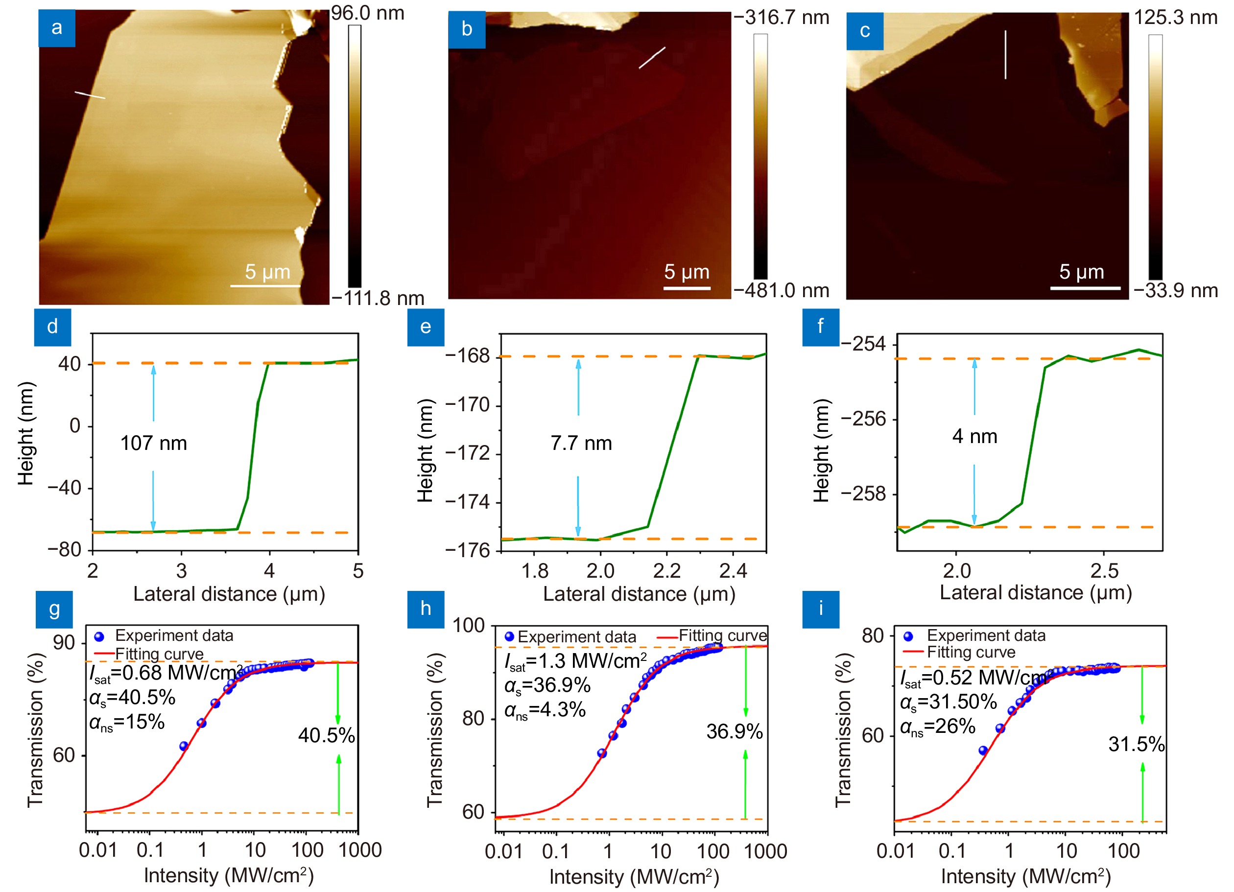
![]()
Figure 1.
SAs generally exhibit traditional intensity-related light transmittance. In detail, most of low-intensity lights are absorbed, while high-intensity lights pass through with low loss. This light intensity-dependent absorption characteristic can be theoretically described by the following formula,
where α exhibits the total absorption of material, αns is non-saturable loss, αs is modulation depth, I is light intensity, Isat is saturation intensity. The insertion loss (IL) of SA is able to be calculated by αns. In the experiment, the traditional balanced twin detector technique is applied to measure the saturated absorption of materials. Using a MLFL whose pulse duration is 200 fs and repetition rate is 110 MHz at 1550 nm as a seed source, the stable illuminant for measurement is obtained. The mode-locked pulses are divided into two channels of light with synchronous and adjustable intensity through a variable optical attenuator and a 3 dB coupler, which are used as test light and reference light respectively. The reference light can be directly measured by an optical power meter, while the test light is measured after passing through the sample. The blue dots in Fig. 1(g) is the data collected from 107 nm-SnS2 SA. After theoretical fitting with formula (1) through red line, the exact values of various nonlinear parameters in formula (1) are determined. From Fig. 1(g), the Isat, αs and αns of 107 nm-SnS2 SA are 0.68 MW/cm2, 40.5% and 15%. Similarly, the Isat, αs and αns of 7.7 nm- and 4 nm-SnS2 SAs are 1.3 MW/cm2, 36.9%, 4.3% (Fig. 1(h)) and 0.52 MW/cm2, 31.5%, 26% (Fig. 1(i)).
Results and discussion
Experimental setup
The components of the experimental device are shown in Fig. 2, including a 980 nm laser diode (LD), erbium-doped fiber (EDF), a SnS2 SA, a 980/1550 wavelength division multiplexer (WDM), isolator (ISO), a polarization controller (PC) and a 80/20 optical coupler (OC). LD provides pump light for the entire system, its maximum output power is 630 mW. WDM is used to synthesize a bunch of 980 nm pump light and 1550 nm light running in the cavity on a single fiber. After the excitation of pump light with high power density, 40 cm-EDF achieves the sufficient particle number reversal state, generating oscillating laser. The SnS2 SA is the key optical modulation device in the cavity, fine tuning the PC to alter the polarization state of the laser and improve the laser quality. The ISO is used to ensure the consistency of the propagation direction of the ring laser. The OC delivers 20% of the intra-cavity laser to the outside of the cavity for real-time observation of the laser performance. The instruments used to measure the properties of QSFL are spectrometer (Yokogawa AQ6370C), spectrum analyzer (Agilent E4402B), and oscilloscope (Tektronix DPO3054).
![]()
Figure 2.
When 107 nm-SnS2 SA is applied to the system, the performance of the QSFL is summarized in Fig. 3. At this time, the pump power (Ppump) of the laser is adjusted to the maximum, which is 630 mW. The pulse duration (τ) of a single pulse displayed on the oscilloscope is 484.7 ns as shown in Fig. 3(a). From the RF spectrum in Fig. 3(b), the fundamental frequency (Frep) of pulse is ~240 kHz, the signal-to-noise ratio (SNR) is up to 50 dB. RF spectrum within a bandwidth of 2 MHz in illustration indicates that the QSFL works well. The spectrum of QSFL in Fig. 3(c) reveals that the wavelength is centered at 1530.6 nm. The standard deviation of output power (Pout) monitoring within 8 hours in Fig. 3(d) is 0.493 mW, which emphasized the constancy of the laser. When the Ppump is regulated, the traditional change trends of corresponding τ, Frep, Pout and pulse energy (Ep) are respectively shown in Fig. 3(e) and 3(f). It is found that the threshold value of laser is 212 mW. The adjustment ranges of τ and Frep are 0.485–1.4 μs and 141–241 kHz. The maximum of Pout is 12.7 mW, and the corresponding Ep is 52.6 nJ.
![]()
Figure 3.
Next, the other two kinds of materials are also used to realize the Q-switched pulse under the same experimental conditions. For the Q-switched pulse under the same experimental conditions. For the QSFL using 7.7 nm-SnS2 SA, the τ is 492.6 ns at the same pump power as shown in Fig. 4(a), which is slightly inferior to the laser based on 107 nm-SnS2 SA. The standard deviation of Pout monitoring within 8 hours in Fig. 4(b) is 0.52 mW. From Fig. 4(c), the threshold value of laser is 276 mW, the τ and Frep are adjustable in the range of 0.493–0.844 μs and 162–240 kHz respectively. From Fig. 4(d), the maximum Pout and Ep are 14.3 mW and 59 nJ.
![]()
Figure 4.
Similarly, the performances of QSFL employing 4 nm-SnS2 SA are recorded in Fig. 5. The τ of the laser at the Ppump of 630 mW is 503.3 ns as shown in Fig. 5(a). The standard deviation of Pout within 8 hours is acknowledged in Fig. 5(b) as 0.543 mW. In Fig. 5(c), the adjustment range of τ and Frep are revealed as 0.503–1.25 μs and 123–248 kHz. The boot threshold of laser is 180 mW. As show in Fig. 5(d), the maximum of Pout and Ep are obtained when the Ppump takes the maximum value of 630 mW, which are 11.3 mW and 45.7 nJ. In addition, each material has been repeatedly tested, eliminating the possibility of experimental error within our capabilities.
![]()
Figure 5.
The performance of three different QSFLs adopting distinct SAs are summarized in Table 1. First of all, it is found that the nonlinear behavior of materials with different thickness is distinct. In terms of modulation depth, the 107 nm-SnS2 owns the best performance. This may be related to the relaxation time. Generally, the material with larger relaxation time is beneficial to the enhancement of the modulation depth. Due to the large specific surface area and/or the presence of multiple edges shortening the lifetime of free carriers
| SA | αs/Isat(MW/cm2) | Threshold(mW) | τ(μs) | Frep (kHz) | Stability (mW) | Pout(mW) | Ep(nJ) |
| 107 nm-SnS2 | 40.5%/0.68 | 212 | 0.485−1.4 | 141−241 | 0.493 | 12.7 | 52.6 |
| 7.7 nm-SnS2 | 36.9%/1.3 | 276 | 0.493−0.844 | 162−240 | 0.52 | 14.3 | 59 |
| 4 nm-SnS2 | 31.5%/0.52 | 180 | 0.503−1.25 | 123−248 | 0.543 | 11.3 | 45.7 |
Table 1. The performance of three different QSFLs adopting distinct SA.
The effect of SA with different nonlinearity on the performance of corresponding lasers is also obvious. The experimental results show that the output power based on SA with 40.5% modulation depth is the most stable (standard deviation: 0.493 mW), this is due to SA with high modulation depth can promote the stability of the system according to the previous research
Currently, passive QSFLs based on various SAs have been extensively studied. Table 2 compares the performance of lasers based on several widely used SAs. By comparison, we find that SnS2 SA seems to have some advantages in the realization of short pulse. Both the laser realized in ref
| Materilas | αs (%) | ∆λ/λ(nm) | Frep(kHz) | τ(μs) | Pout/Ppump(mW) | Threshold(mW) | Ep(nJ) | SNR(dB) | Refs. |
| Graphene | − | 0.02/1539.6 | 10.36−41.8 | 3.89 | <1.2/65 | 13.5 | 28.7 | 30 | ref. |
| BP | 18.55 | 0.2/1562.87 | 6.983−15.78 | 13.2 | ~1.5/195 | 50 | 94.3 | 45 | ref. |
| WS2 | 2.53 | −/1560 | 47.03~77.93 | 3.96 | 6.41/650 | 400 | 1179.4 | 54.2 | ref. |
| MoS2 | 2 | −/1551.2 | 8.77−43.47 | 3.3 | 5.91/227 | 18.9 | 160 | 50 | ref. |
| SnS2 | 3.15 | 0.03/1532.7 | 172.3−233.0 | 0.510 | 9.33/632 | 290 | ~40 | 50 | ref. |
| SnS2 | 40.5 | 4.3/1530.6 | 141−241 | 0.485 | 12.7/630 | 180 | 45.7 | 50 | This work |
Table 2. Comparison of QSFL based on various SAs.
Carrier mobility and electronic structure calculations of multi-layer SnS2 with different thickness
Structure optimization and band structure calculations were performed based on density functional theory (DFT) as implemented in the Vienna ab-initio simulation package (VASP)
The relaxation time related to the carrier mobility μ, and μ in 2D semiconductor film of finite thickness is calculated based on the deformation potential
where F is a crossover function that bridges 2D and 3D
here, erf() represents the error function, and the summation over integer n is due to quantum confinement along the z-direction (finite thickness direction). Ω(n) is defined as
Weff is the effective thickness of the film, which can be calculated analytically by assuming a square-well confinement potential.
In Eq. (2), DA is the deformation potential, which is calculated from its definition
where Eg is the band gap. Our DFT calculations indicate that the electron mobility is thickness-dependent, it increases with increased thickness, and converges to bulk state when the thickness reaches either-layer as shown in Fig. 6.
![]()
Figure 6.
The intrinsic carrier concentration is rather sensitive to the band gap and less sensitive to the variation of the effective mass. Due to the decreased band gap of SnS2 with increased thickness, our DFT calculations in Table 3 clearly reveal that the intrinsic carrier concentration is significantly increased as the thickness increases, thus corresponding to the enhanced modulation depth.
| Thickness | Band gap | nix (m−2) |
| 1-Layer | 1.57 eV | 2.44×10+3 |
| 2-Layer | 1.52 eV | 6.74×10+3 |
| 4-Layer | 1.39 eV | 1.13×10+5 |
| 6-Layer | 1.34 eV | 4.73×10+5 |
| 8-Layer | 1.27 eV | 1.79×10+6 |
Table 3. The intrinsic carrier concentration (
Conclusions
In short, three kinds of SnS2 with different thickness are characterized in terms of nonlinearity and used to realize the Q-switched pulses. The SnS2 SA is prepared through the combination of CVT and ME to double guarantee the high quality of materials. By comparing the nonlinear performance of SnS2 SA with different thickness, it is found that the thicker material shows higher modulation depth due to the influence of large relaxation time. Because of the combined effect of scattering loss and relaxation time, the initial transmission and thickness do not show a simple linear trend, but there is an optimal value. In addition, the saturation intensity is related to the initial transmittance of the material. Furthermore, the performances of the QSFLs with these three kinds of SA are compared. It is found that large modulation depth is beneficial to the stability of the laser, and at the same time, it seems to have a weak advantage in the realization of ultrashort pulse. A small saturation intensity of SA tends to make the laser have a small start threshold. In addition, combined with previous research, SnS2 seems to have inherent advantages and potential in achieving ultrashort pulse. These results clarify the thickness-dependent nonlinear optical properties of SnS2, and the impact of various optical nonlinear parameters of SA on the performance of the corresponding laser, which provides a meaningful reference for further research on the application of SnS2 or similar TMDs materials in nonlinear optics.
References
[1] Observation and optimization of 2 μm mode-locked pulses in all-fiber net anomalous dispersion laser cavity. Opto-Electron Adv, 3, 200001(2020).
[2] Passively Q-switched Tm/Ho composite laser. Opto-Electron Adv, 3, 190031(2020).
[3] CVD-grown MoSe2 with high modulation depth for ultrafast mode-locked erbium-doped fiber laser. Nanotechnology, 29, 394002(2018).
[4] Mid-infrared all-fiber gain-switched pulsed laser at 3 μm. Opto-Electron Adv, 3, 190032(2020).
[5] Nonlinear optical properties of MoS2-WS2 heterostructure in fiber lasers. Opt Express, 27, 6689-6699(2019).
[6] WS2 as a saturable absorber for ultrafast photonic applications of mode-locked and Q-switched lasers. Opt Express, 23, 11453-11461(2015).
[7] Q-switched fiber laser operating at 1.5 μm based on WTe2. Chin Opt Lett, 17, 020006(2019).
[8] Nonlinear optical properties of WSe2 and MoSe2 films and their applications in passively
[9] Revealing the plasmon coupling in gold nanochains directly from the near field. Opto-Electron Adv, 2, 180030(2019).
[10] 8 ns fiber laser
[11] Large energy mode locking of an erbium-doped fiber laser with atomic layer graphene. Opt Express, 17, 17630-17635(2009).
[12] Atomic-layer graphene as a saturable absorber for ultrafast pulsed lasers. Adv Funct Mater, 19, 3077-3083(2009).
[13] Optical modulators with 2D layered materials. Nat. Photonics, 10, 227-238(2016).
[14] MoTe2 saturable absorber with high modulation depth for erbium-doped fiber laser. J Lightwave Technol, 37, 3100-3105(2019).
[15] Sub-200 fs soliton mode-locked fiber laser based on bismuthene saturable absorber. Opt Express, 26, 22750-22760(2018).
[16] Broadband nonlinear optical response in multi-layer black phosphorus: an emerging infrared and mid-infrared optical material. Opt Express, 23, 11183-11194(2015).
[17] Synthesis of high quality silver nanowires and their applications in ultrafast photonics. Opt Express, 27, 16440-16448(2019).
[18] Large-area tungsten disulfide for ultrafast photonics. Nanoscale, 9, 1871-1877(2017).
[19] MoS2 saturable absorber prepared by chemical vapor deposition method for nonlinear control in Q-switching fiber laser. Chin Phys B, 27, 084211(2018).
[20] Two-dimensional SnS2 nanoplates with extraordinary high discharge capacity for lithium ion batteries. Adv Mater, 20, 4269-4273(2008).
[21] SnS2 nanosheets for Er-doped fiber lasers. ACS Appl Nano Mater, 3, 674-681(2020).
[22] Passively mode-locked Er-doped fiber laser based on SnS2 nanosheets as a saturable absorber. Photonics Res, 6, 72-76(2018).
[23] Tin disulfide-an emerging layered metal dichalcogenide semiconductor: materials properties and device characteristics. ACS Nano, 8, 10743-10755(2014).
[24] High-performance top-gated monolayer SnS2 field-effect transistors and their integrated logic circuits. Nanoscale, 5, 9666-9670(2013).
[25] Vertically aligned graphene-like SnS2 ultrathin nanosheet arrays: excellent energy storage, catalysis, photoconduction, and field-emitting performances. J Phys Chem C, 116, 9319-9326(2012).
[26] Dissipative soliton generation in Er-doped fibre laser using SnS2 as a saturable absorber. Appl Phys Express, 12, 102008(2019).
[27] Dual-wavelength mode-locked erbium-doped fiber laser based on tin disulfide thin film as saturable absorber. J Appl Phys, 125, 243104(2019).
[28] Noise-like mode-locked Yb-doped fiber laser in a linear cavity based on SnS2 nanosheets as a saturable absorber. Appl Optics, 58, 6007-6011(2019).
[29] Thickness-dependent ultrafast photonics of SnS2 nanolayers for optimizing fiber lasers. ACS Appl Nano Mater, 2, 2697-2705(2019).
[30] Passively Q-switched erbium-doped fiber laser based on SnS2 saturable absorber. Opt Mater Express, 7, 3934-3943(2017).
[31] Thickness-dependent structure and properties of SnS2 thin films prepared by atomic layer deposition. Jpn J Appl Phys, 56, 031201(2017).
[32] 322 single crystals and vertical nanostructures: role of edges. In Proceedings of the 43rd International Conference on Infrared, Millimeter, and Terahertz Waves (IRMMW-THz, 2018) (IEEE, 2018);http://doi.org/10.1109/IRMMW-THz.2018.8509909.
[33]
[34] Evanescent-light deposition of graphene onto tapered fibers for passive Q-switch and mode-locker. IEEE Photonics J, 4, 1295-1305(2012).
[35] Mechanically exfoliated black phosphorus as a new saturable absorber for both Q-switching and Mode-locking laser operation. Opt Express, 23, 12823-12833(2015).
[36] Q-switched fiber laser based on transition metal dichalcogenides MoS2, MoSe2, WS2, and WSe2. Opt Express, 23, 26723-26737(2015).
[37] Widely-tunable, passively Q-switched erbium-doped fiber laser with few-layer MoS2 saturable absorber. Opt Express, 22, 25258-25266(2014).
[38] Efficiency of ab-initio total energy calculations for metals and semiconductors using a plane-wave basis set. Comput Mater Sci, 6, 15-50(1996).
[39] Efficient iterative schemes for
[40] Projector augmented-wave method. Phys Rev B, 50, 17953-17979(1994).
[41] From ultrasoft pseudopotentials to the projector augmented-wave method. Phys Rev B, 59, 1758-1775(1999).
[42] Generalized gradient approximation made simple. Phys Rev Lett, 77, 3865-3868(1996).
[43] A consistent and accurate
[44] Special points for Brillouin-zone integrations. Phys Rev B, 13, 5188-5192(1976).
[45] Hybrid functionals based on a screened Coulomb potential. J Chem Phys, 118, 8207-8215(2003).
[46] 46J Chem Phys 124, 219906 (2006).
[47] Deformation potentials and mobilities in non-polar crystals. Phys Rev, 80, 72-80(1950).
[48]
[49] High-mobility transport anisotropy and linear dichroism in few-layer black phosphorus. Nat Commun, 5, 4475(2014).
[50] Calculated carrier mobility of h-BN/
[51] First-principles calculation of intrinsic carrier mobility of silicene. J Appl Phys, 114, 093712(2013).

Set citation alerts for the article
Please enter your email address
© Copyright 2018-2021 | Chinese Laser Press. All Rights Reserved 沪ICP备15018463号-20